July 2025 · pre-alpha
The first control program
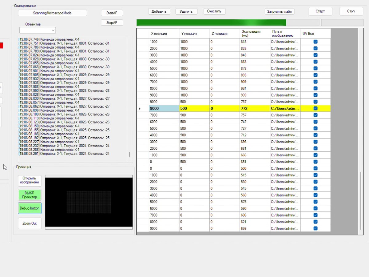
Windows Forms: a table of fields, each with its own position and exposure time — dose sweeps set up by hand.
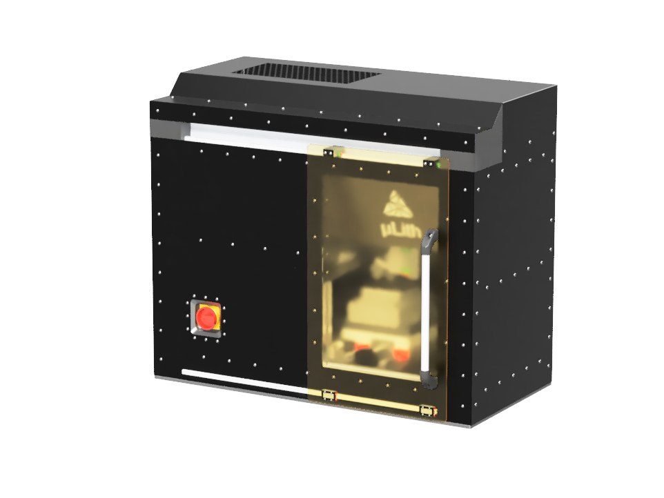
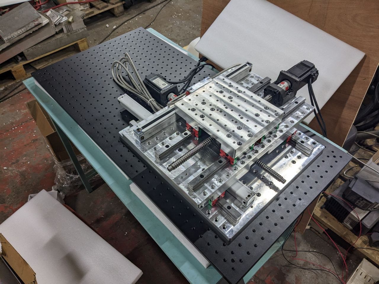
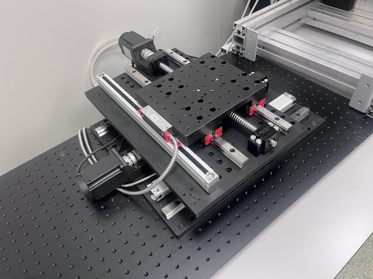
The machine that proved the idea: a DMD projection lithograph that exposes resist on real wafers straight from a GDSII file. Enclosed desktop unit, 440 nm LED, closed-loop XY stage on servo drives and optical scales, a camera looking through the same objective.
Built and working
A TI DLP4710 DMD — 1920 × 1080 micromirrors — is a programmable photomask. Each frame of the layout is projected through a microscope objective onto the resist; the stage steps and stitches frames into one continuous pattern.

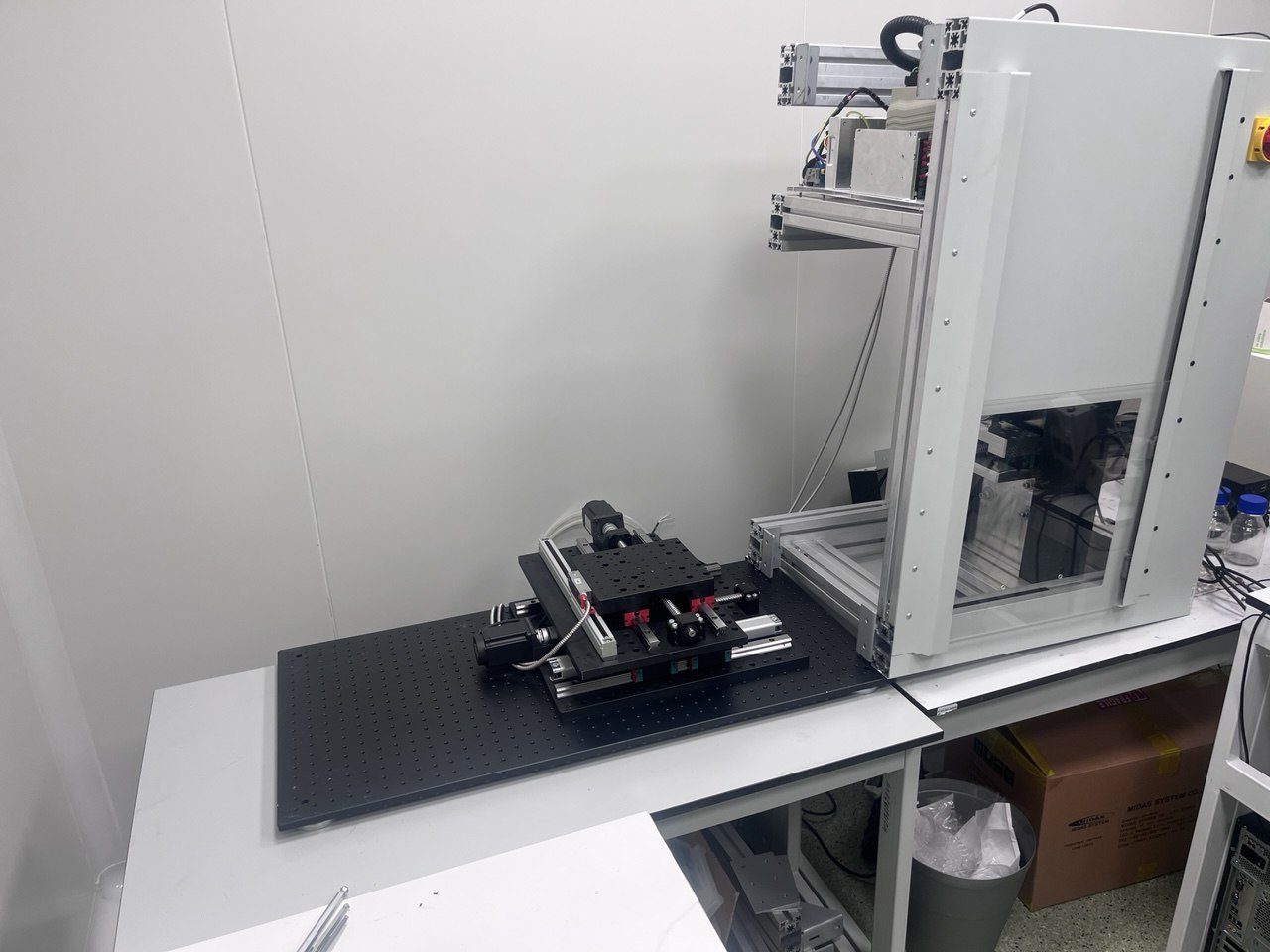
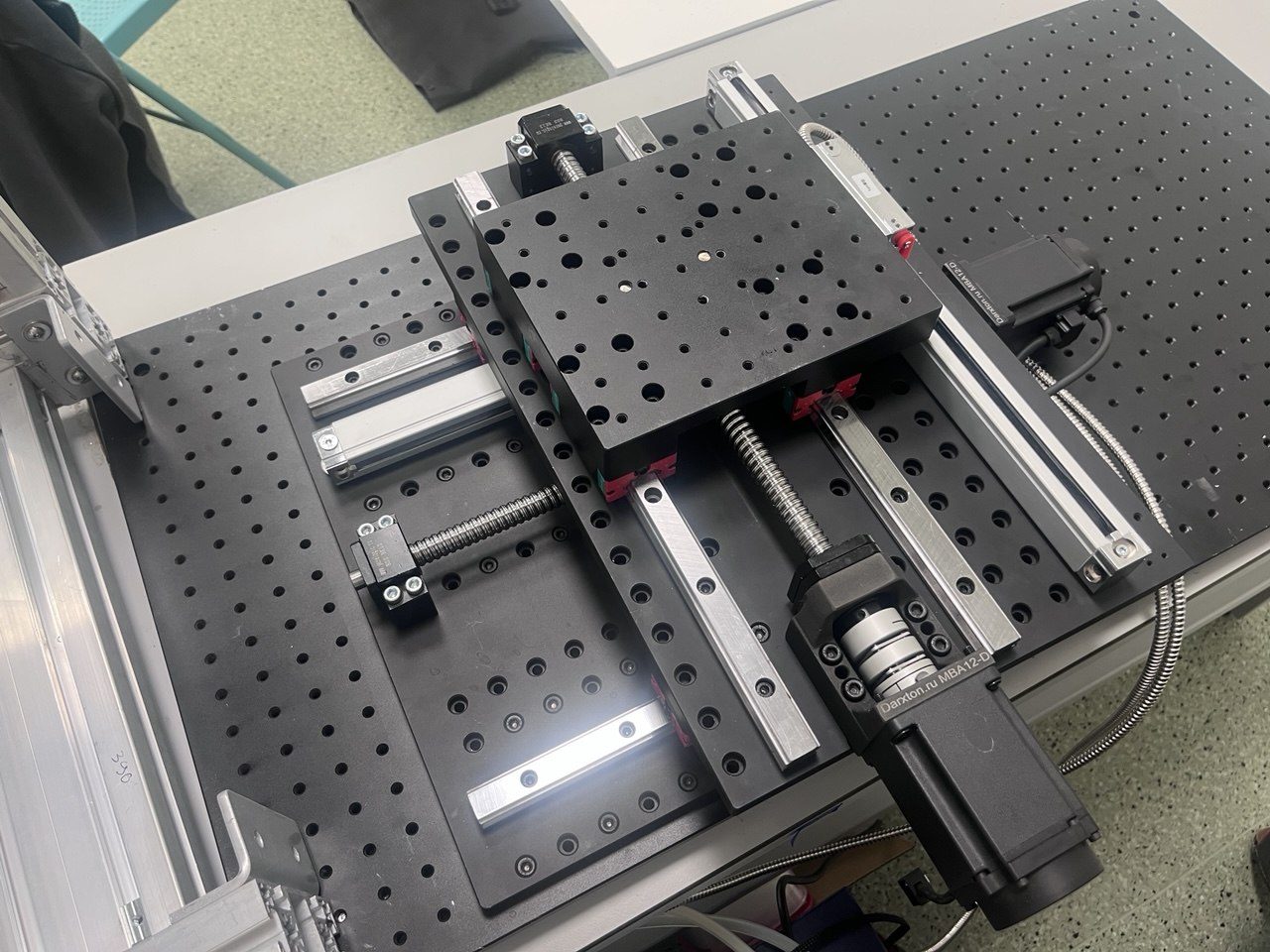
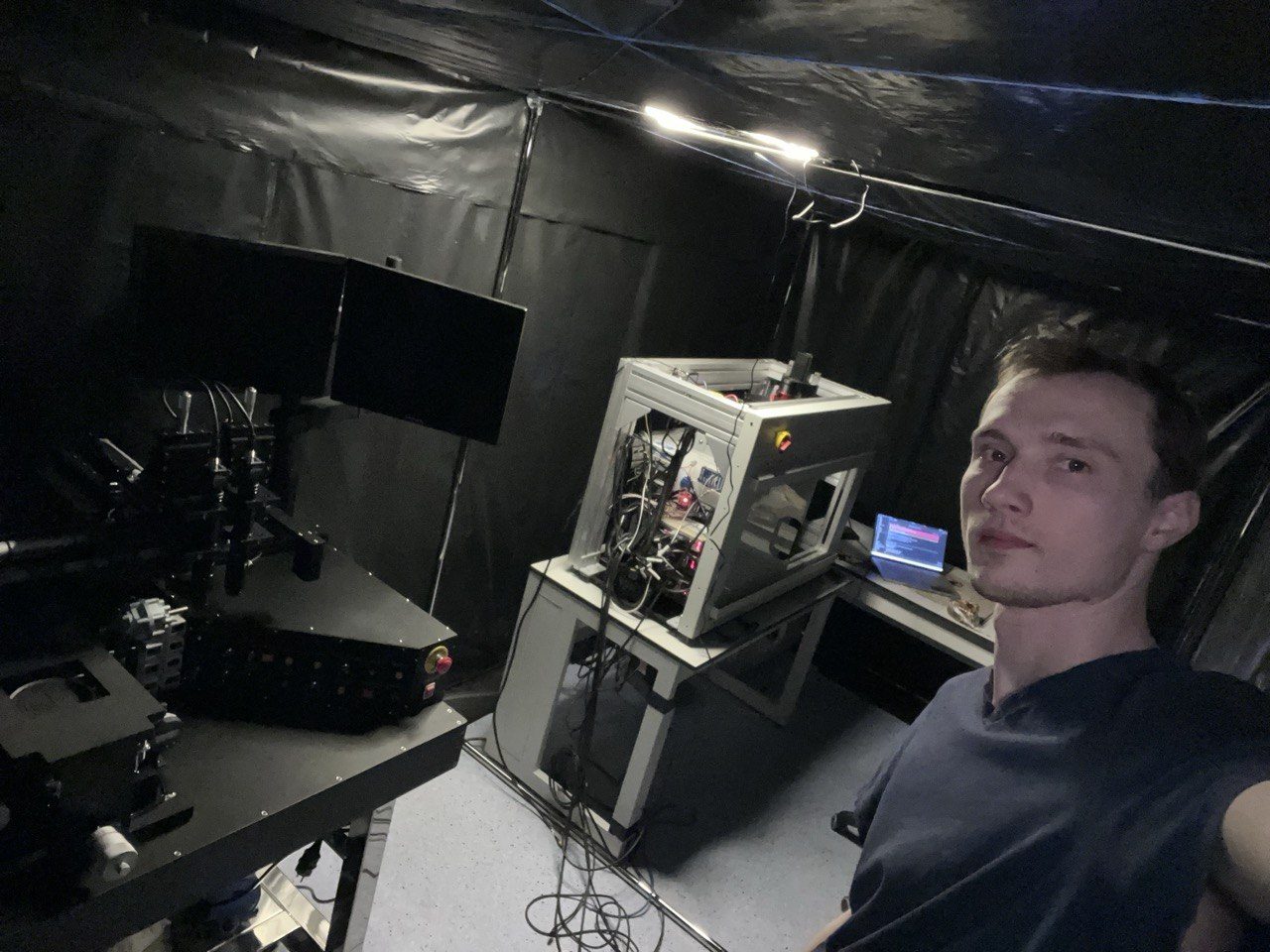
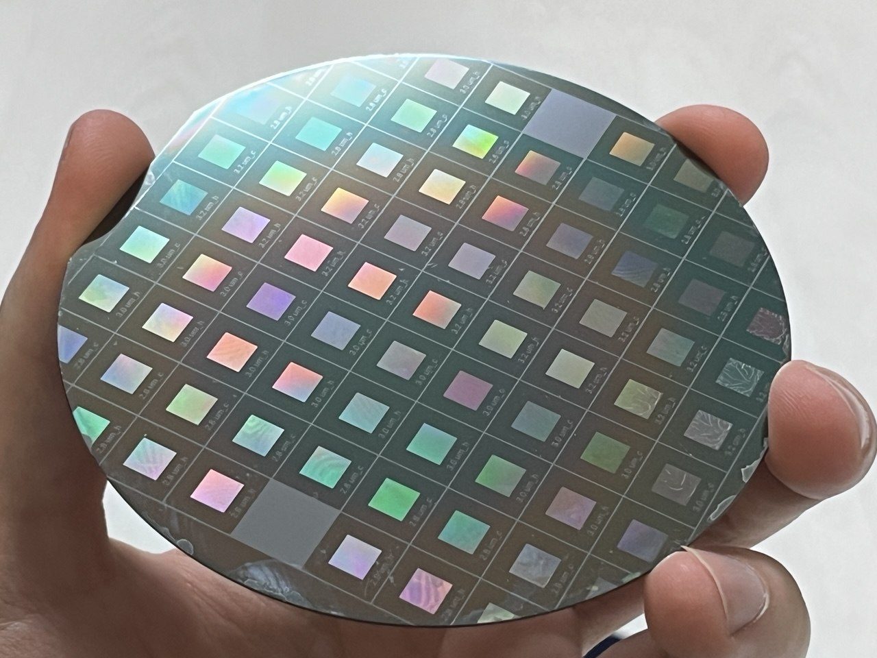
Photographs, not simulations: exposed and developed on Prototype 1.0.
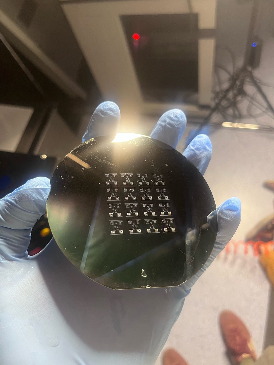
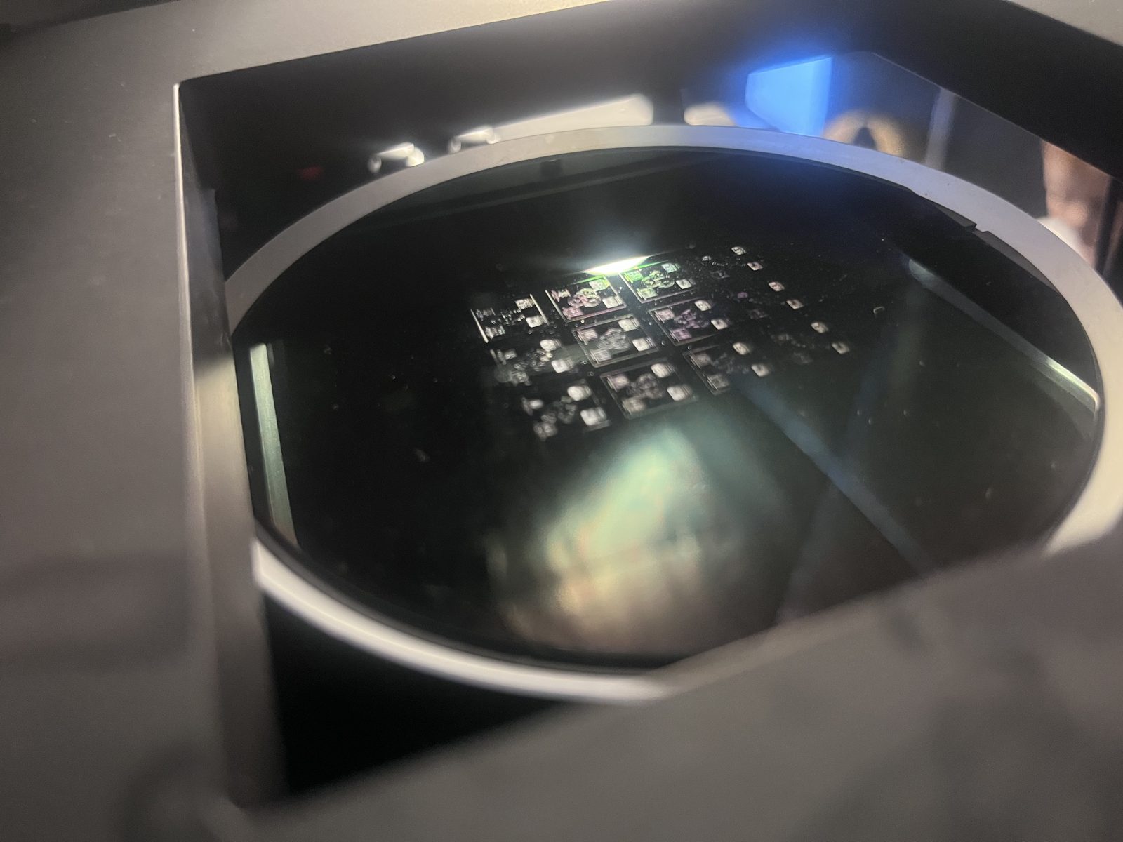
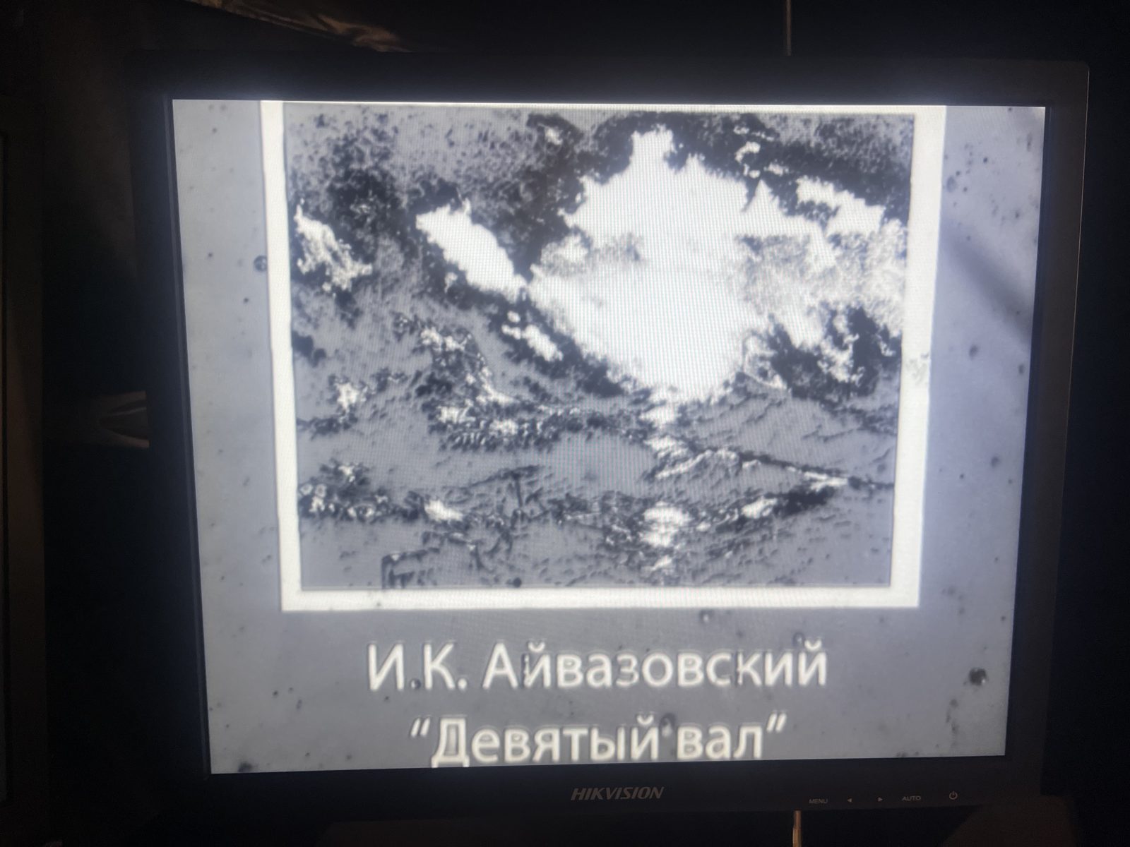
Sub-micron precision here does not come from granite and air bearings. The machine measures its own geometry and illumination with a camera in the wafer plane and cancels them on every field; the software refuses to expose with an uncalibrated objective.


Drag the divider. On the left is the GDSII file that went to the machine; on the right, a photograph of what came out, corrected for perspective so the two line up.
The silicon chip is 25 × 25 mm; the layout on it, a logo with captions and four dithered pictures, takes 20 × 20 mm. One exposure job.
The machine exposes one DMD frame at a time: this chip is 1 869 fields of 0.25 × 0.38 mm, placed side by side by the stage. Switch the picture to Exposure fields and back, and look for the seams.
What ends up in resist depends on development as much as on exposure: developer, time and temperature all change the result. These are samples from process tuning. Works by Magritte and Escher are blurred on both sides: they are still under copyright.
Prototype 2.0. The optical core and software are carried over from Prototype 1.0.
Today it is a single-layer tool: expose, develop, done. If your process needs aligned multilayer now, ask me about the timeline.
Fine-line boards and flex circuits, straight from the layout — same-day iteration.
Channel networks, master molds for PDMS, on-chip electrodes.
Resist patterns for etching, lift-off and plating on Si up to 4″.
Gratings, diffractive elements, waveguide test structures.
On-chip test cells, microelectrode platforms, microbatteries.
No laser class, compact, enclosed — real workflows from GDSII to wafer.
A year of iterations. The pre-alpha ran on a different projector with a first program written in Windows Forms; Prototype 1.0 got its own stage, its own software and a stitched exposure process.
Windows Forms: a table of fields, each with its own position and exposure time — dose sweeps set up by hand.
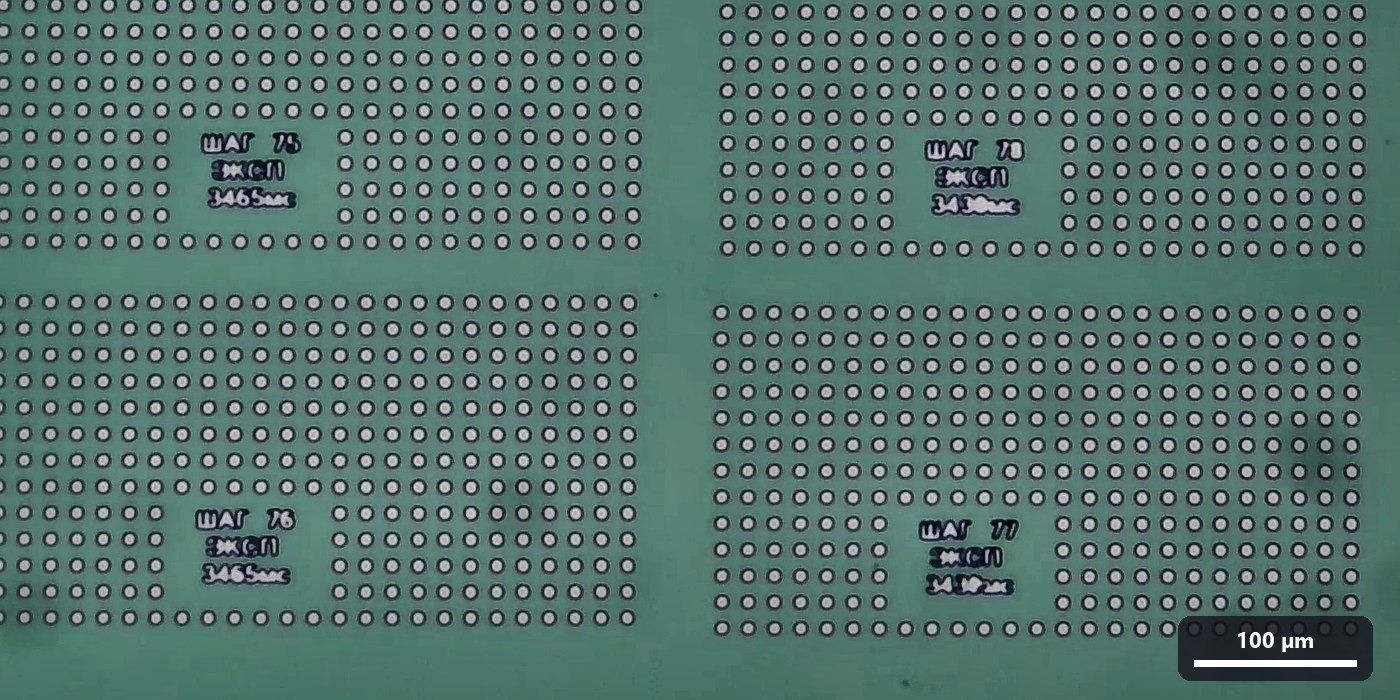
Test arrays in resist, each exposed in a single projected field with no stitching, labelled with its own exposure settings.
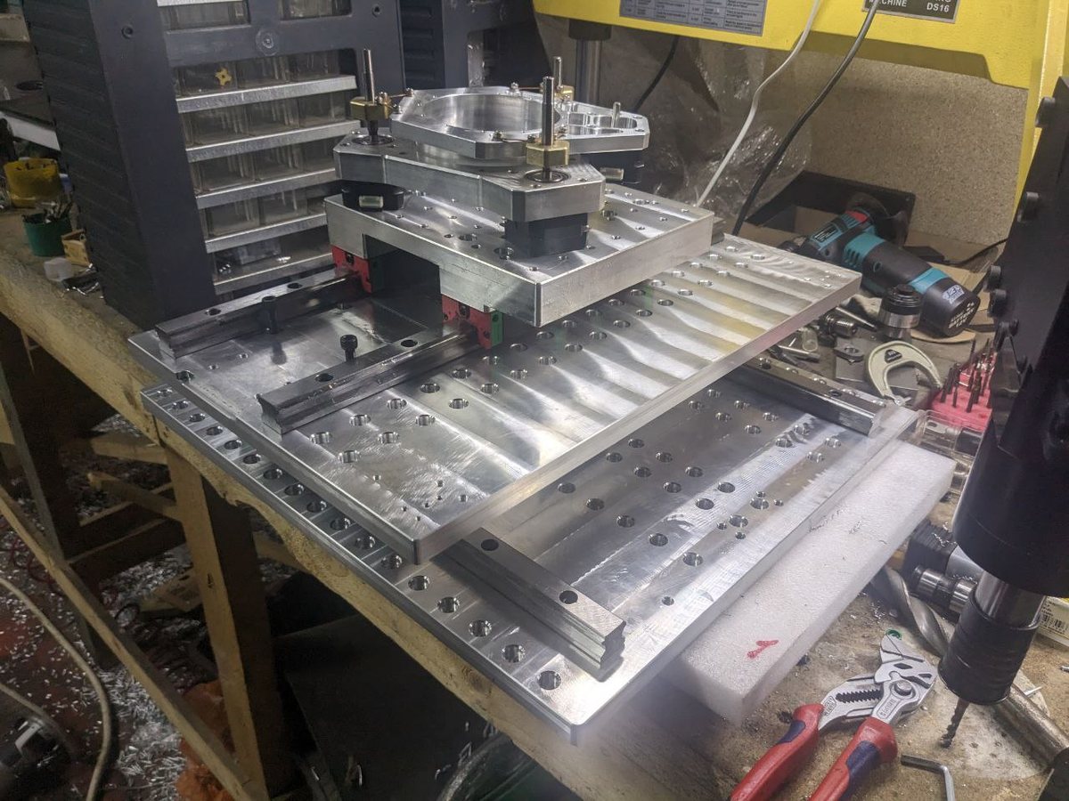
The XY stage on a milling machine: the rotary platform fitted and the mounting plane machined level.
Its own stage on servo drives and optical scales, the QtLithoCAN software, autofocus and a height map, jobs stitched across whole wafers — everything above on this page.
A test chip made of 1 869 exposure fields shows no visible seams.
On the table: a working Prototype 1.0, the Prototype 2.0 design, full documentation and in-house software. A partner brings production, supply chain and market access; deal structure and investment size are open. Demonstrations and sample exposures by arrangement.