Desktop Maskless Lithography
Photolithography straight from a layout file. No photomasks, no mask aligner, no waiting — a design change is a file change.
Two machines, one line of work. Prototype 1.0 is built and working: it exposes real wafers today and runs software written in-house. Prototype 2.0 turns what it taught me into a modular sub-micron motion platform, with lithography as its first instrument.
Prototype 1.0
Built and working
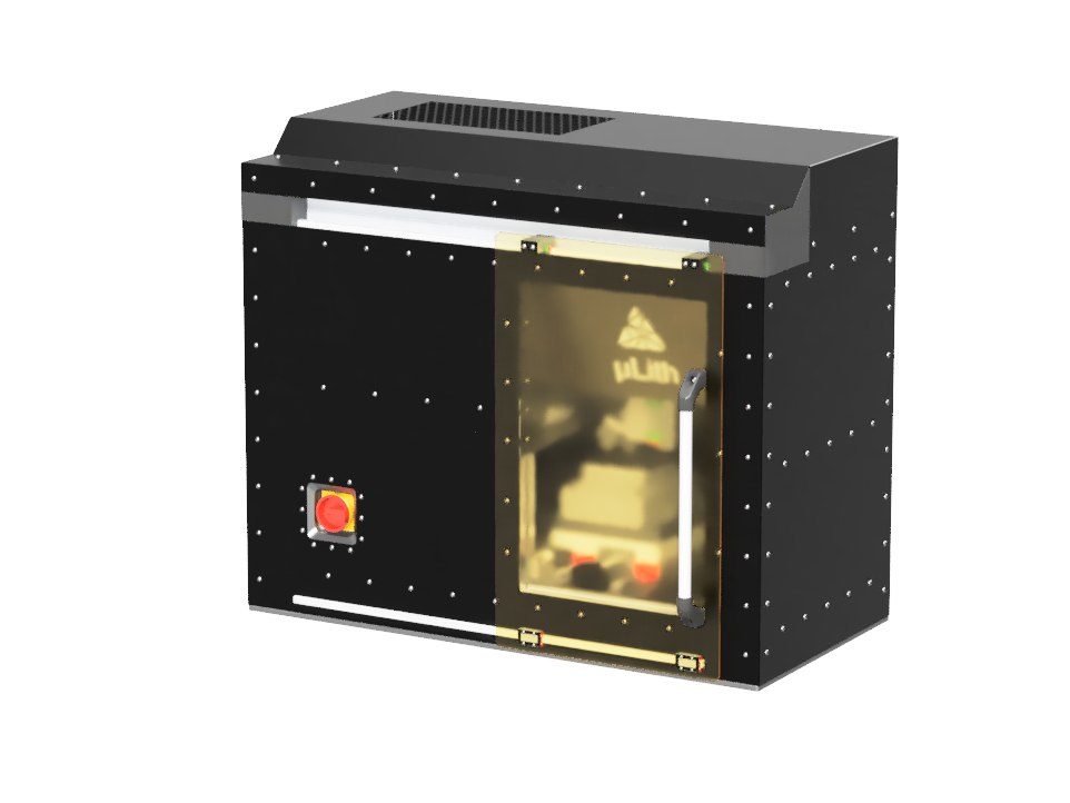
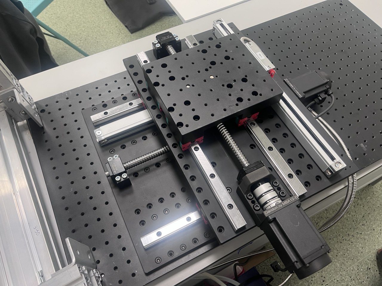
The machine that proved the idea. Enclosed desktop unit: DMD projection head, 440 nm LED, closed-loop XY stage on servo drives and optical scales, a camera looking through the same objective. It exposes resist on real wafers.
How it works
A TI DLP4710 DMD — 1920 × 1080 micromirrors — is a programmable photomask. Each frame of the layout is projected through a microscope objective onto the resist; the stage steps and stitches frames into one continuous pattern.

Prototype 2.0
Modular platform · CAD stage
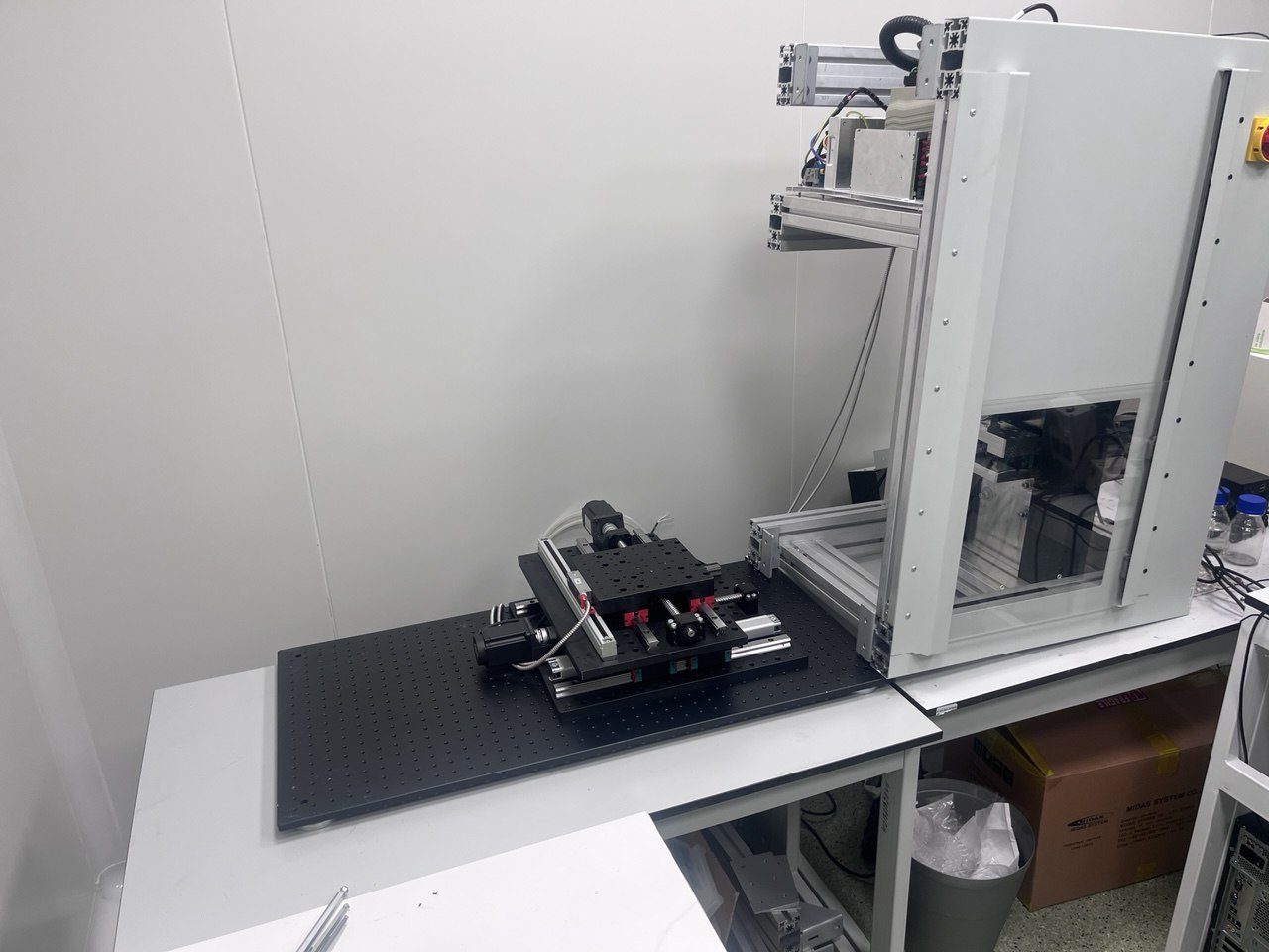
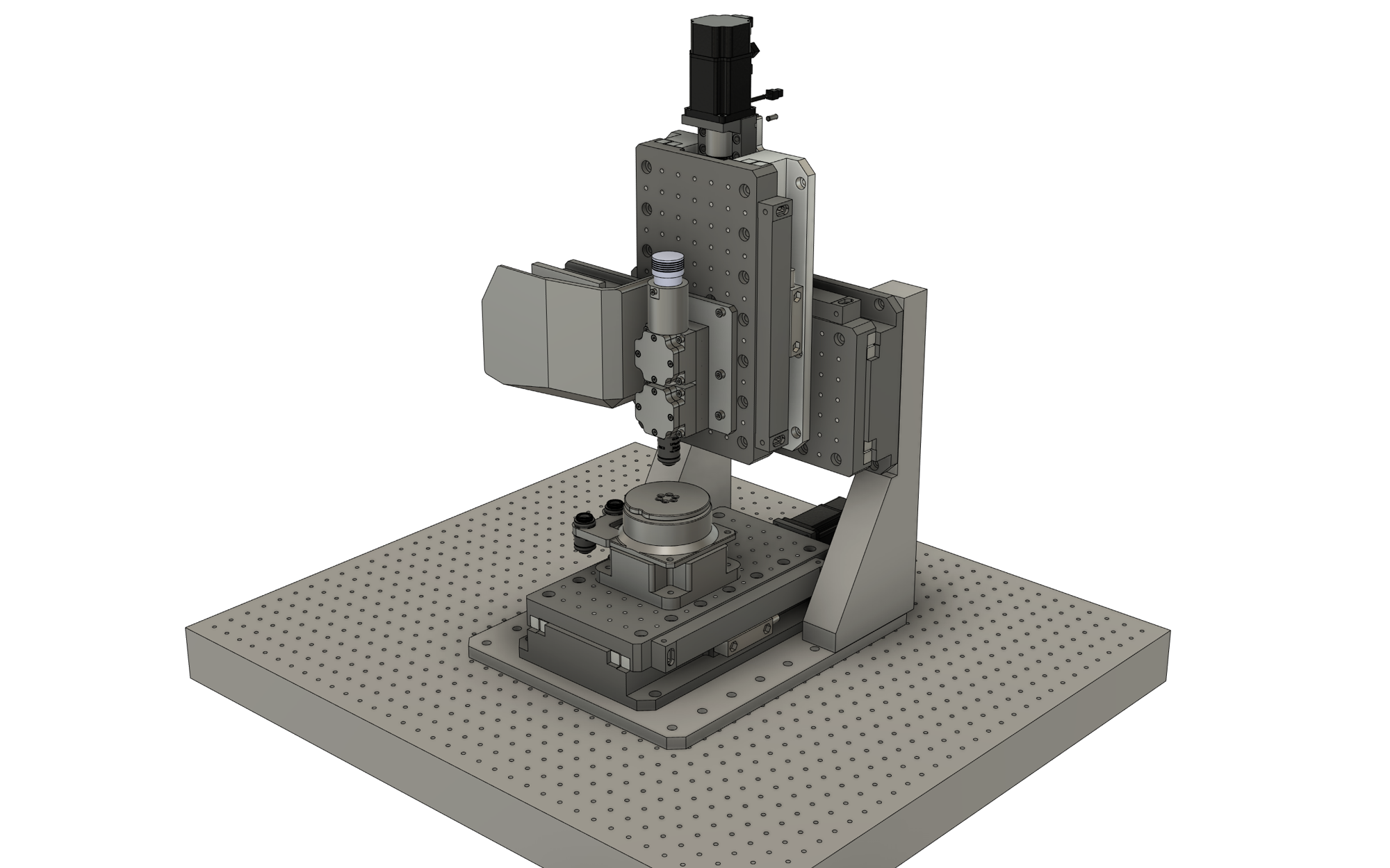
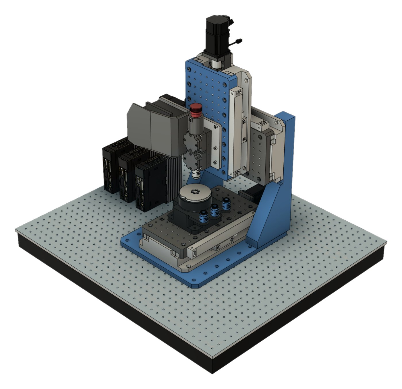
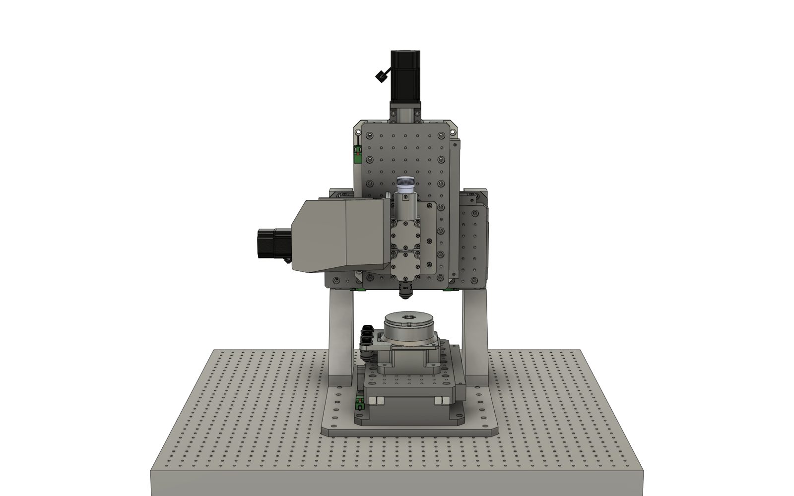
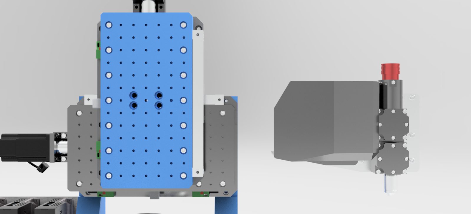
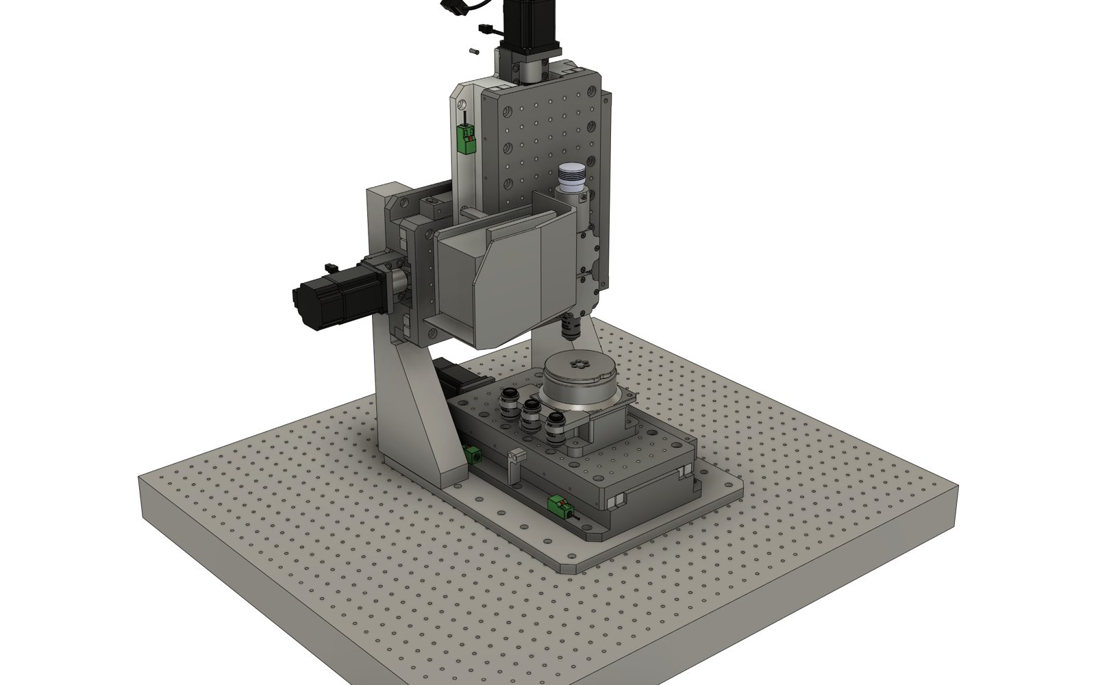
A precision 3-axis motion platform first; lithography is one configuration of it. Three identical linear modules make the XYZ gantry, and everything above the stage bolts to a standard optical-breadboard grid.
Renders with dots are interactive: hover over or tap a part to see what it does.
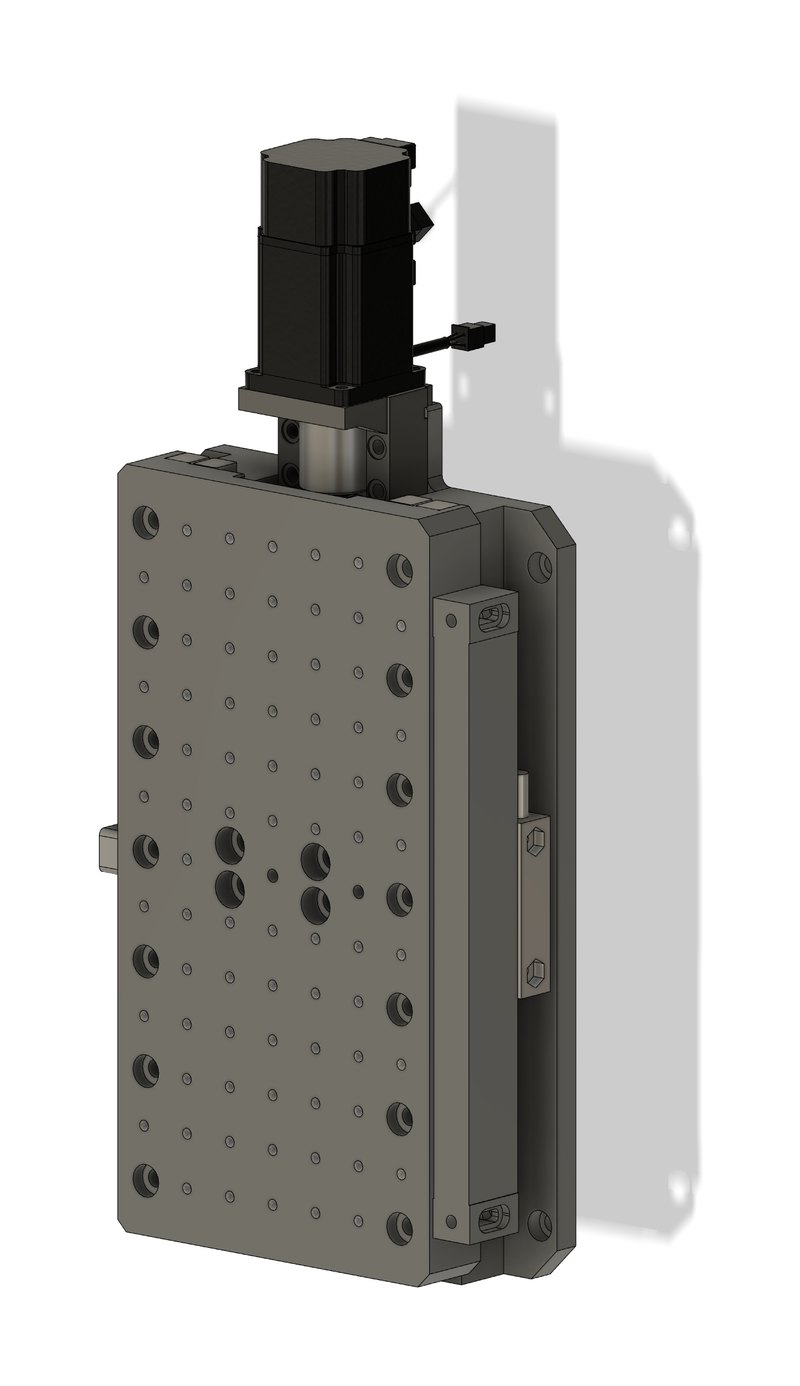
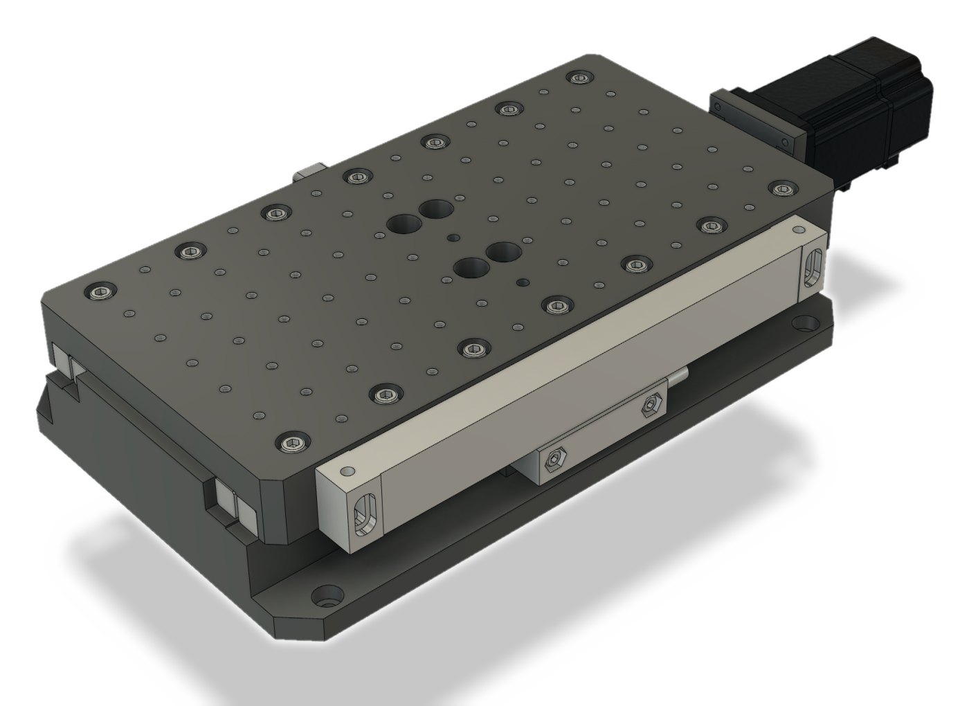
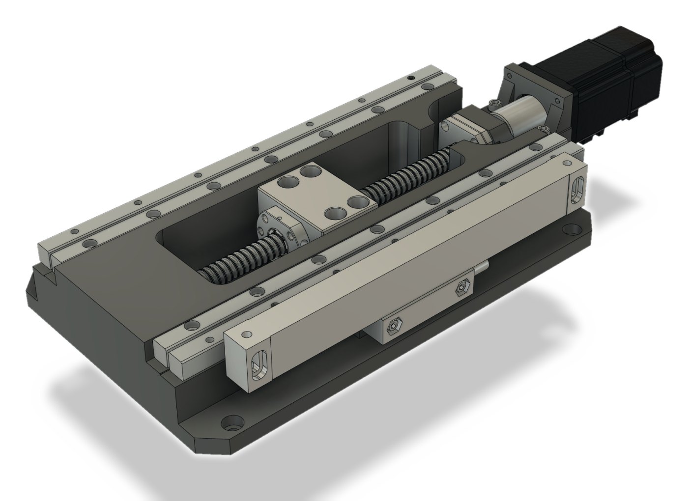
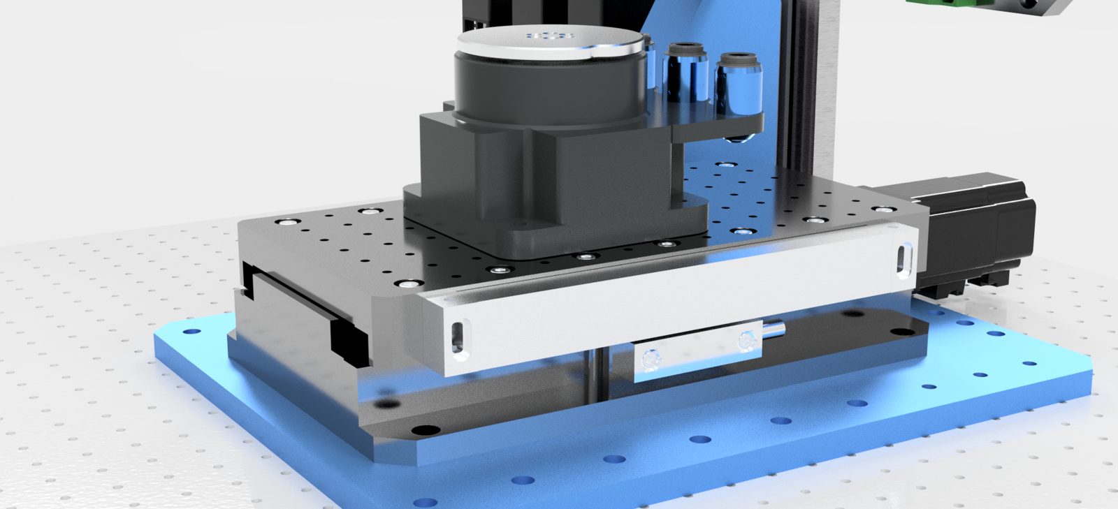
Sub-micron linear module
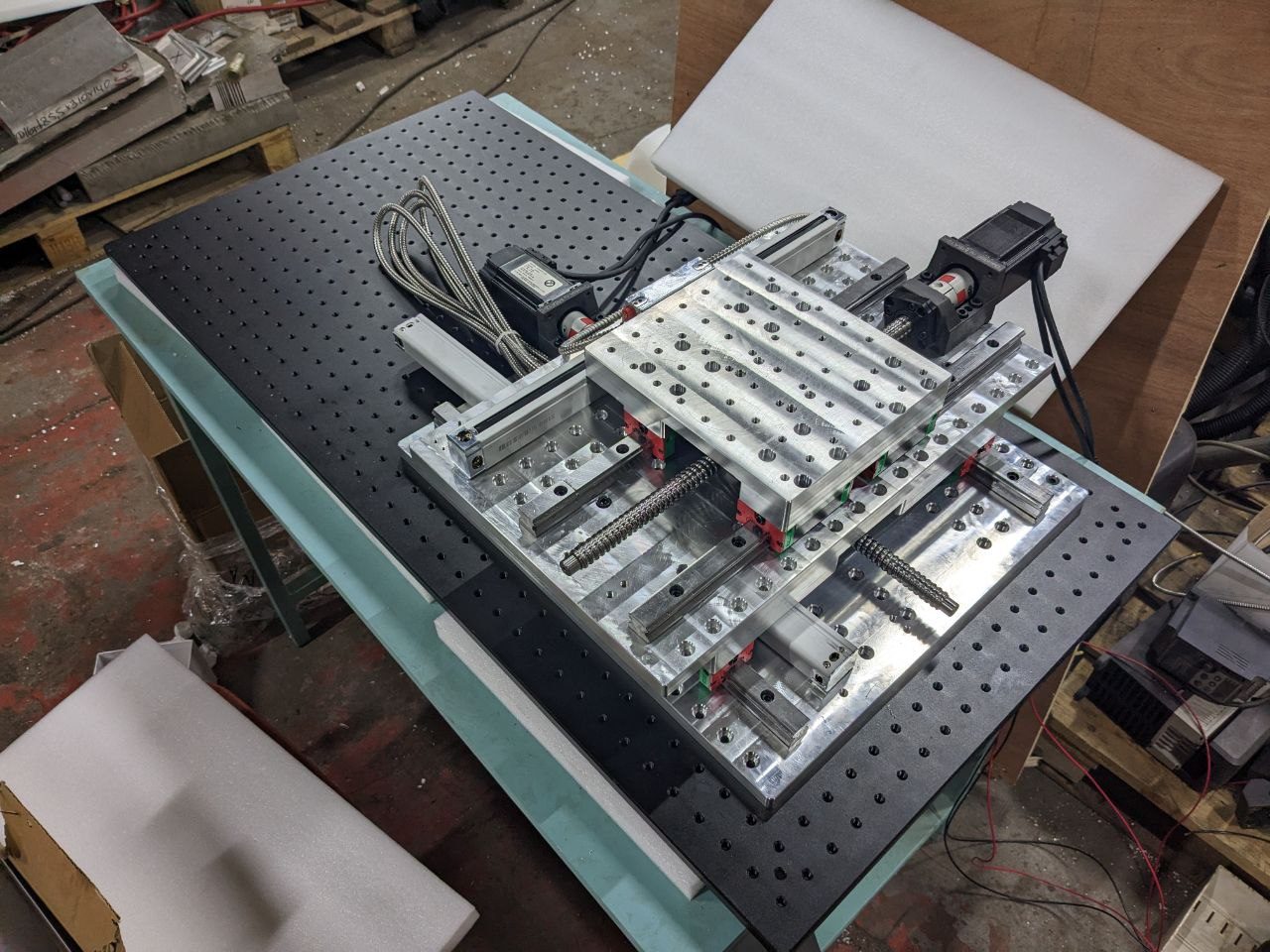
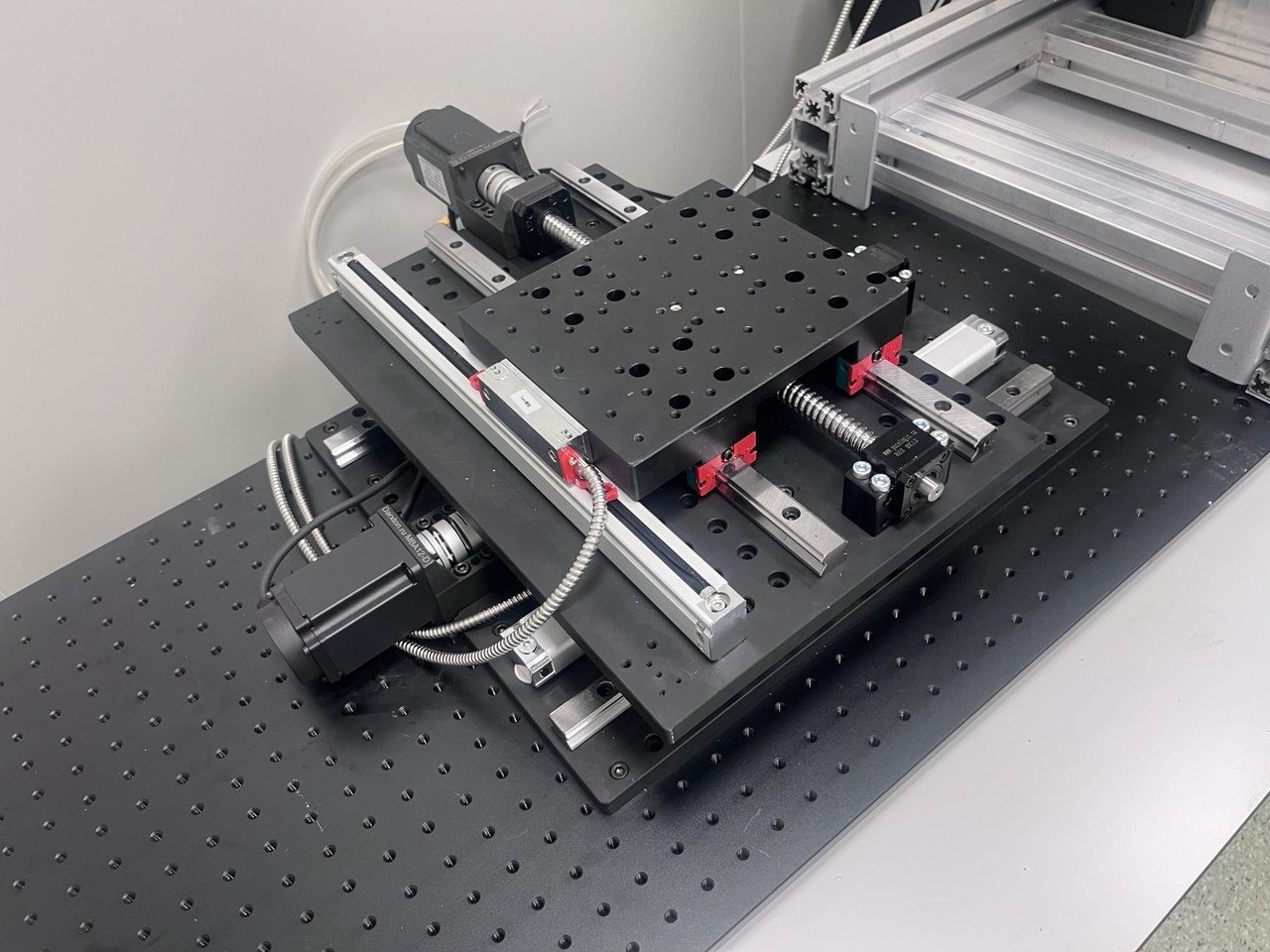
Every axis is the same block: servo drive, ball screw, crossed-roller guides and an optical scale, closed-loop and complete in itself — 100 nm as standard, 2.5 nm as an option. A product line of its own.
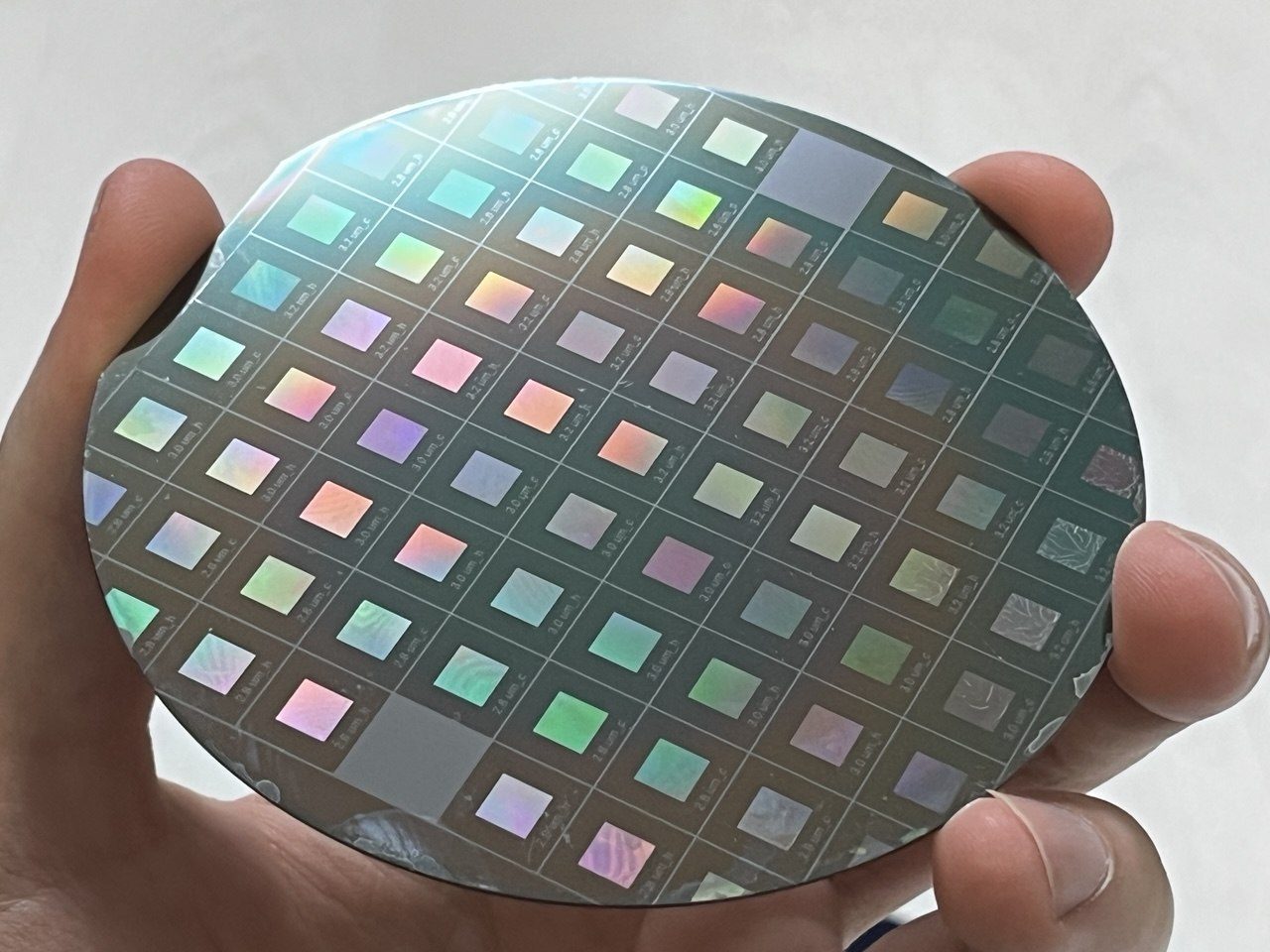
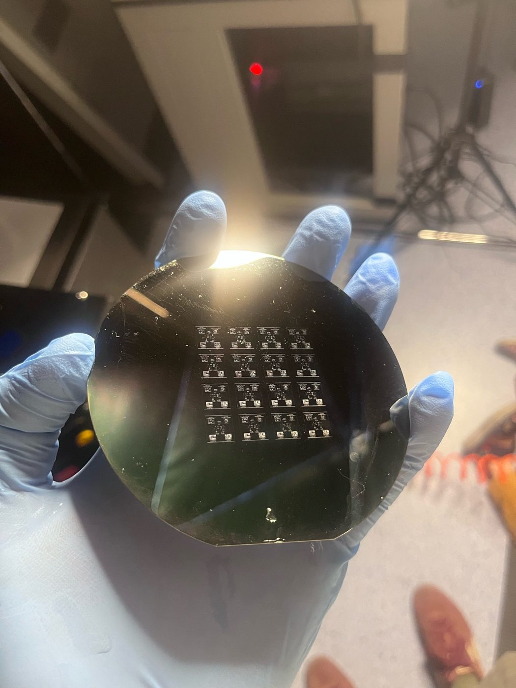
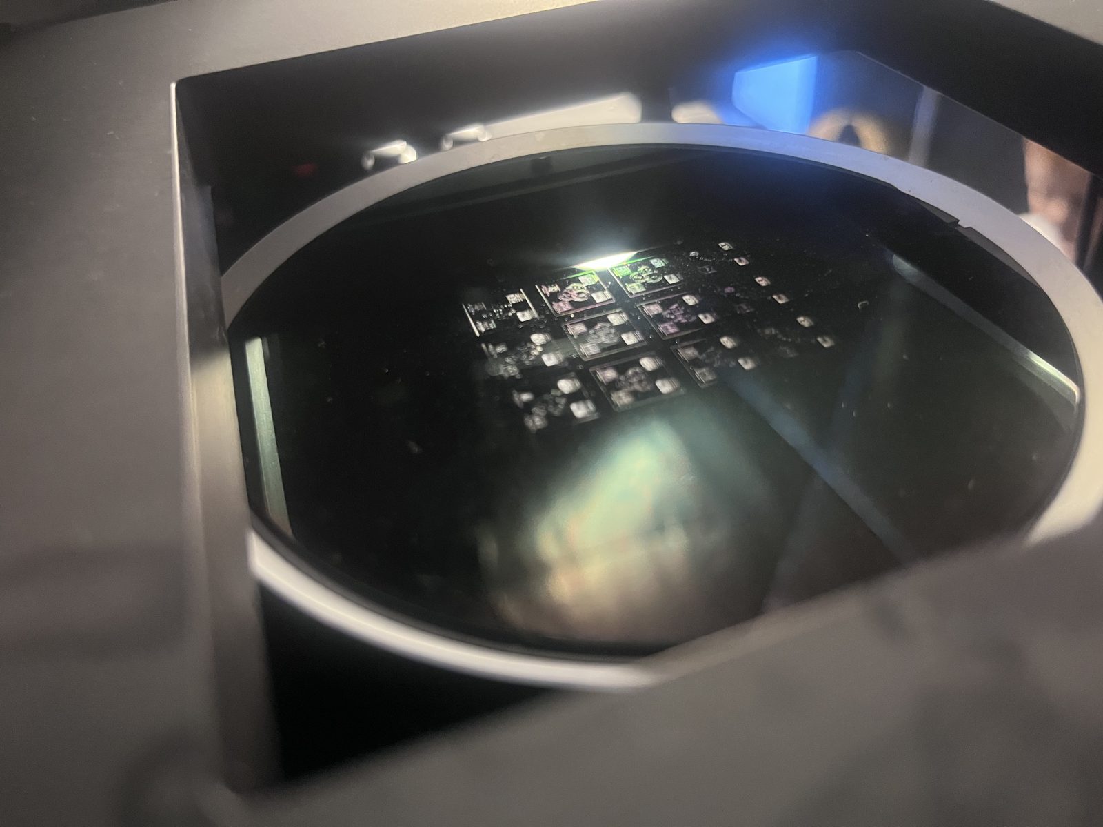
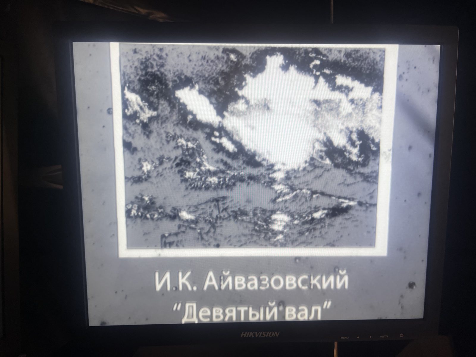
Made on this machine
Photographs, not simulations: exposed and developed on Prototype 1.0.
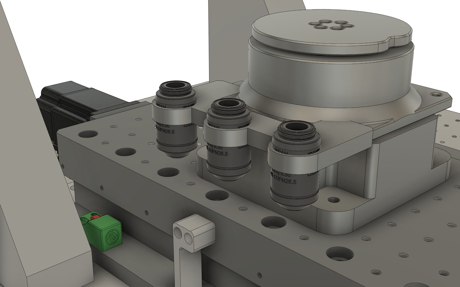
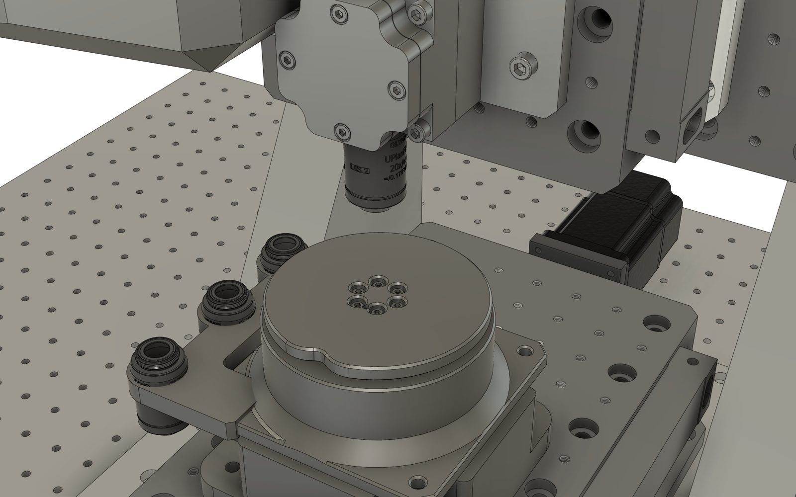
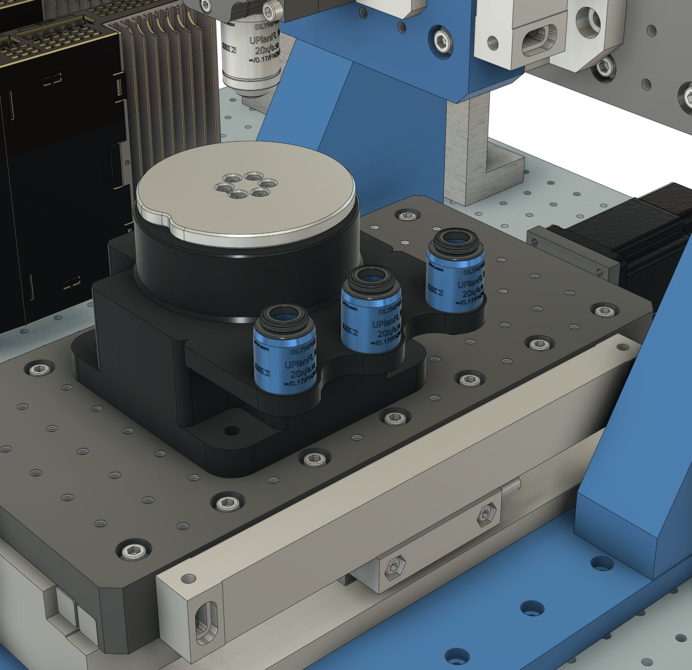
Objectives, chuck, scales
What changes against Prototype 1.0: an open gantry instead of a box, and every part of the optical path made swappable.
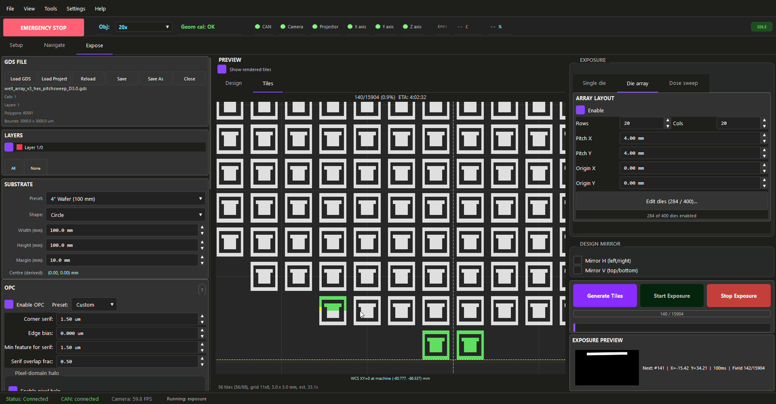
Written in-house, runs the job from layout to wafer
No third-party CAM chain, no licence dependencies. MVP level: everything below runs on the tool today.
What it does
- Native GDSII import, layers, automatic tiling
- Die arrays / step-and-repeat
- OPC assist and focus-exposure matrix
- Two-phase contrast autofocus under red light
- Resist-safe illumination: only blue exposes
- Per-tile exposure time and dose-sweep wafers
- Substrate height map, per-field Z
- CANopen servo motion, exposure interlocks
- Scientific camera pipeline, scale bar per objective
- Project files with stale-tile detection
Target specifications
Prototype 2.0. The optical core and software are carried over from Prototype 1.0.
- Feature size
- 0.7–1 µm typicalmin 0.4 µm, optics & resist dependent
- Exposure area
- 100 × 100 mmscalable to 200 × 200 mm
- Light source
- LED, 440 nm405 nm option · no laser
- XY repeatability
- 0.2 µmclosed loop on optical scales
- Position feedback
- 100 nm scalesdown to 2.5 nm option
- Throughput
- ~2.8 mm²/min @ 1 µm10×; ~0.9 mm²/min @ 0.5 µm (20×)
- Light modulator
- TI DLP4710 DMD1920 × 1080 micromirrors
- Objectives
- 10× / 0.5 · 20× / 0.75interchangeable
- Substrates
- Si up to 4″ · glass · PCB
- Travel X / Y / Z
- ≥100 / ≥100 / 40 mm
- Design input
- GDSII nativeDXF — tuning
- Mounting
- 25 mm grid, M6×1optical-breadboard standard
In development
- Layer-to-layer alignmentrotary vacuum chuck + alignment workflow in software
- Automatic objective changemotorized swap between 10× and 20×
- 405 nm LED optionfor sub-0.5 µm work and broader resist compatibility
- 2.5 nm optical scalesfor repeatability in the 25–50 nm class
Today it is a single-layer tool: expose, develop, done. If your process needs aligned multilayer now, ask me about the timeline.
Precision from calibration
Sub-micron precision here does not come from granite and air bearings. The camera that looks through the objective is also the metrology instrument: the machine measures its own scale, projector rotation and axis squareness, and cancels them on every field. Illumination is flattened pixel by pixel; focus follows a measured height map. The software refuses to expose with an uncalibrated objective.
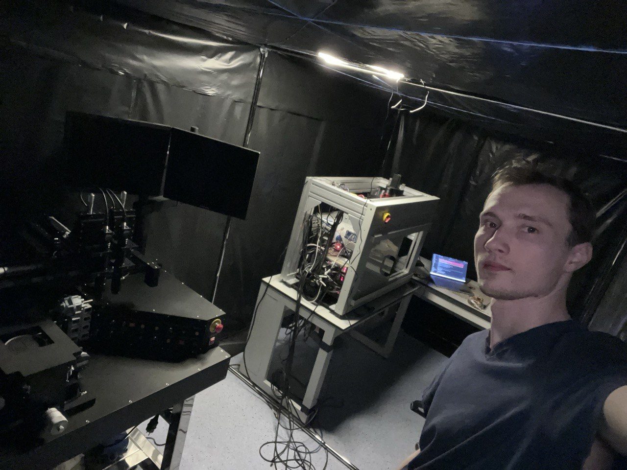
One engineer
Mechanics, optics, electronics and software — designed, built and brought to working condition by one person.
Where it fits
One base, different instruments
Electronics & PCB
Fine-line boards and flex circuits, straight from the layout — same-day iteration.
Microfluidics
Channel networks, master molds for PDMS, on-chip electrodes.
MEMS & sensors
Resist patterns for etching, lift-off and plating on Si up to 4″.
Photonics
Gratings, diffractive elements, waveguide test structures.
Battery R&D
On-chip test cells, microelectrode platforms, microbatteries.
Education & labs
No laser class, compact, enclosed — real workflows from GDSII to wafer.
Looking for a manufacturing partner and investor
On the table: a working Prototype 1.0, the Prototype 2.0 design, full documentation and in-house software. A partner brings production, supply chain and market access; deal structure and investment size are open. Demonstrations and sample exposures by arrangement.