Calibration: the machine measures itself
A camera goes on the stage with its sensor facing up, in the plane where the wafer would be. The projector then draws straight onto the sensor, so the software sees exactly what the resist would get — and measures geometry, dose and stitching from it. The same procedure carries over to Prototype 2.0.
The payoff: tolerances move from hardware into software. Parts, rails and optics do not have to be perfect, and the machine does not have to be assembled perfectly — whatever is left is measured and cancelled. That keeps the parts cheaper and the build simpler.


What calibration changes
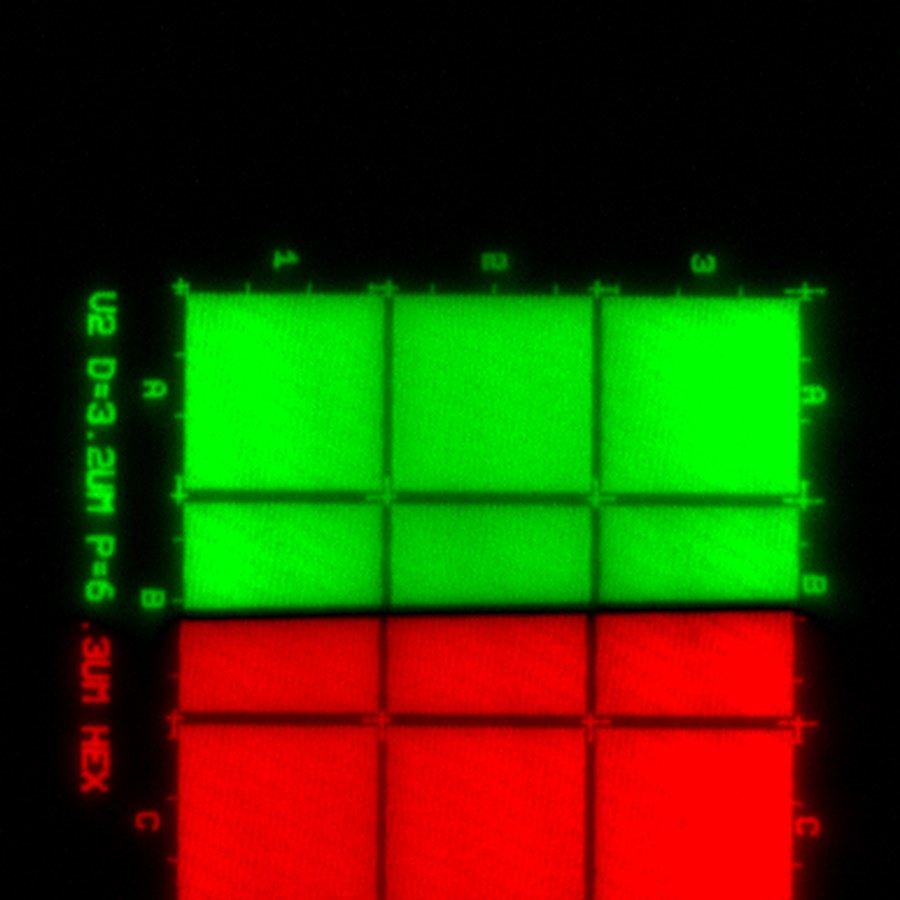
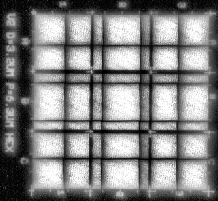
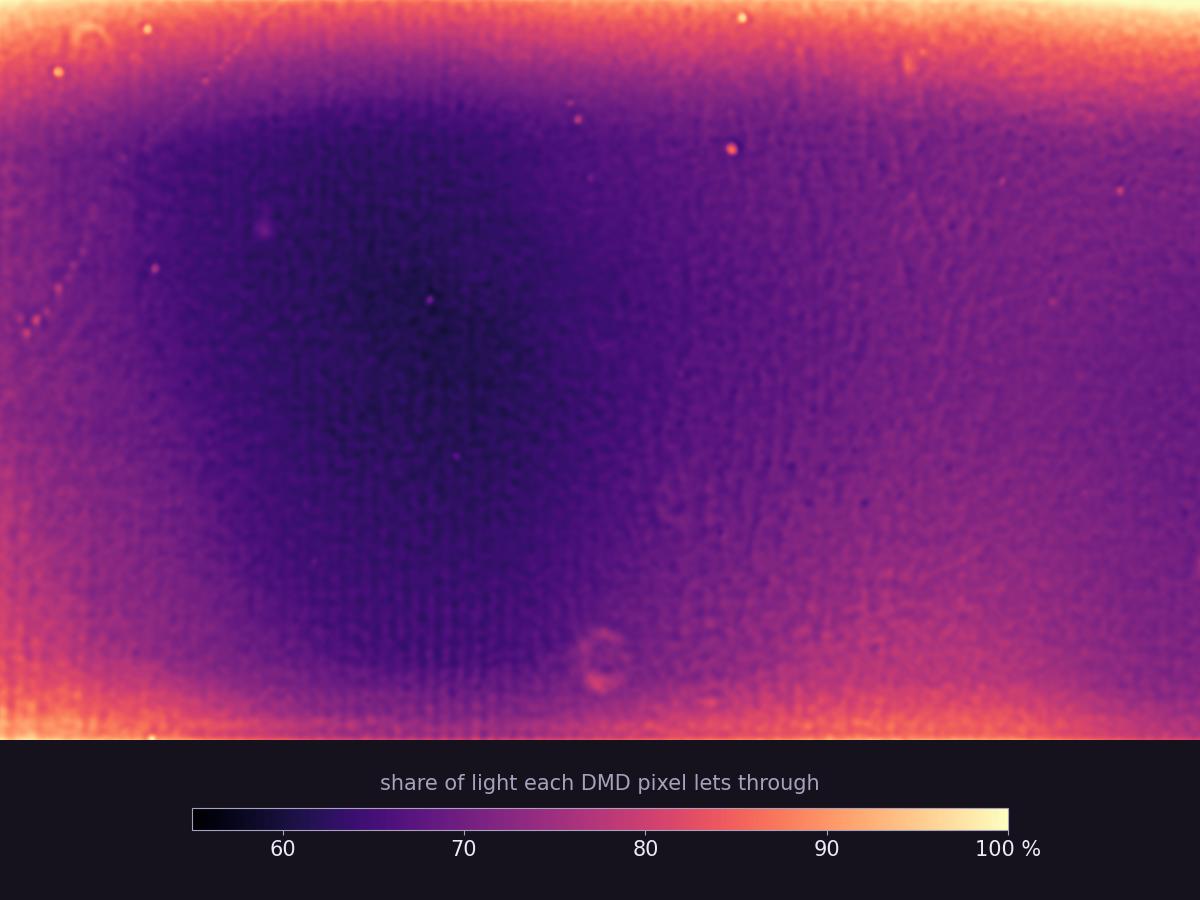
Drag the divider. Measured sides are camera frames taken in the wafer plane (one sensor pixel is 3.75 µm on the substrate). The compensated side of the white field illustrates the correction algorithm on that same frame.
One square frame exposed at 25 stage positions and stacked into one image. Before: projector rotation against the stage and the rails’ shear show as tilted squares with uneven gaps. After: every move goes through the measured 2 × 2 correction.
Geometry: one 2 × 2 matrix
Projector rotation against the stage, the shear between the X and Y rails and the scale of each axis are measured together and applied to every move. Sub-micron placement at the edge of a 100 mm wafer needs the angle to about 4 arcseconds.
Dose: a per-pixel mask
The camera maps illumination across the field; the software turns it into an attenuation mask on the DMD and adjusts exposure time per tile. The camera then measures the result again, and the mask is refined until the field is flat to within 2–3 %.
Illumination flat to within 2–3 %
| Objective | Before | After | Darkest vs brightest |
|---|---|---|---|
| 10× | 48.7 % | 97.8 % | −2.2 % |
| 20× | 63.0 % | 97.9 % | −2.1 % |
| 40× | 70.0 % | 97.2 % | −2.8 % |
Uniformity here is the dimmest 2 % of the field — or the darkest corner, whichever is worse — over the brightest 2 %, measured through the objective and averaged over 256 frames. Each objective gets its own mask, refined pass by pass until a pass stops improving it. July–August 2026.
Looking for a manufacturing partner and investor
On the table: a working Prototype 1.0, the Prototype 2.0 design, full documentation and in-house software. A partner brings production, supply chain and market access; deal structure and investment size are open. Demonstrations and sample exposures by arrangement.