ILIA SIDOROVMASKLESS LITHOGRAPHY Get in touch
DESKTOP · MASKLESS · DIRECT FROM GDSII

Desktop Maskless Lithography

Photolithography straight from a layout file. No photomasks, no mask aligner, no waiting — a design change is a file change.

Two machines, one line of work. Prototype 1.0 is built and working: it exposes real wafers today and runs software written in-house. Prototype 2.0 turns what it taught me into a modular sub-micron motion platform, with lithography as its first instrument.

Prototype 1.0 · a full exposure job, ×15
GDSII
native input · no masks
1920 × 1080
DMD micromirrors
440 nm
LED source · no laser
Full closed-loop
servo axes on optical scales
Built

Prototype 1.0

Built and working

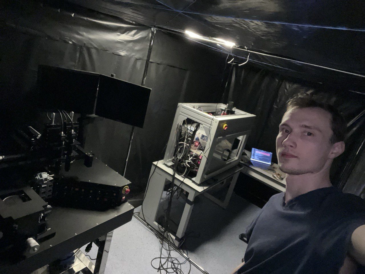
The machine that proved the idea. Enclosed desktop unit: DMD projection head, 440 nm LED, closed-loop XY stage on servo drives and optical scales, a camera looking through the same objective. It exposes resist on real wafers.
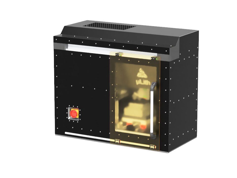
The enclosure: head, stage and electronics in one light-tight box with an E-stop.
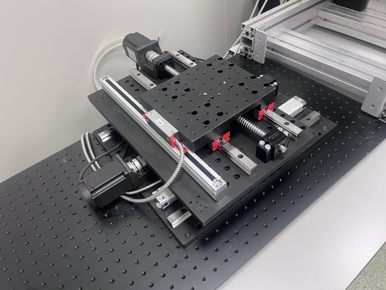
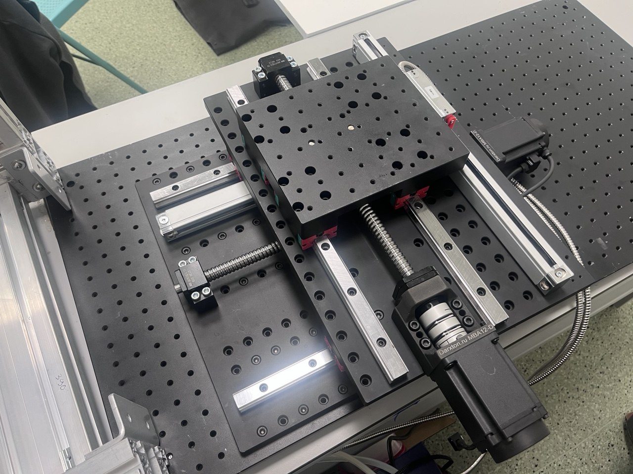
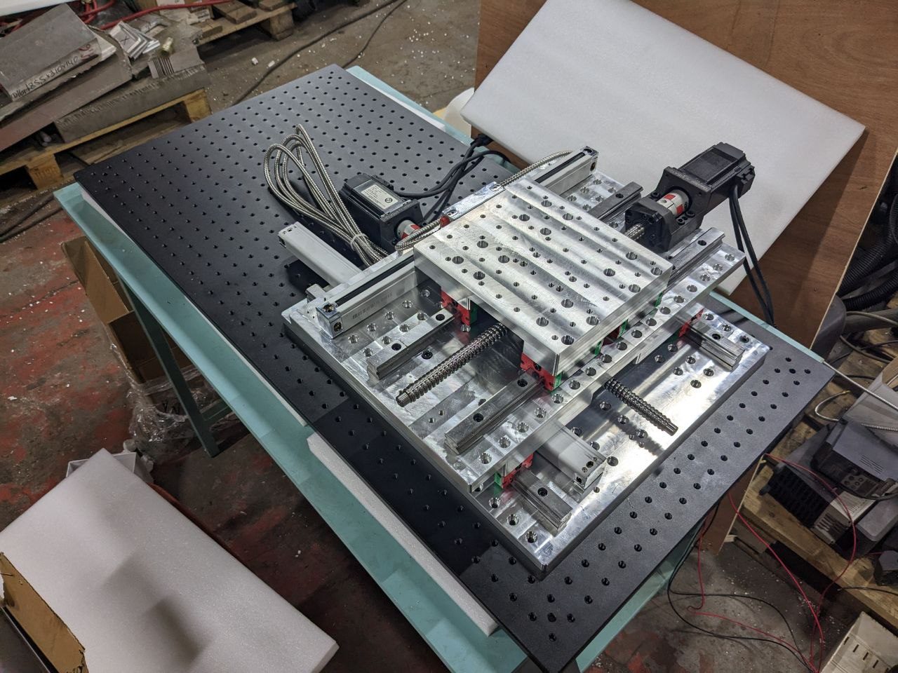
XY stage during assembly.
After anodizing, assembled.

How it works

A TI DLP4710 DMD — 1920 × 1080 micromirrors — is a programmable photomask. Each frame of the layout is projected through a microscope objective onto the resist; the stage steps and stitches frames into one continuous pattern.

Optical scheme
Projection path; the camera shares it.
Exposure in progress.
Autofocus: the objective travels in Z.
Exposure seen from the side.
Stage and enclosure frame, taken apart.
Servo drives and optical scales on both axes.
Rotary platform under the chuck — the first step towards layer-to-layer alignment.
Results

Made on this machine

Photographs, not simulations: exposed and developed on Prototype 1.0.
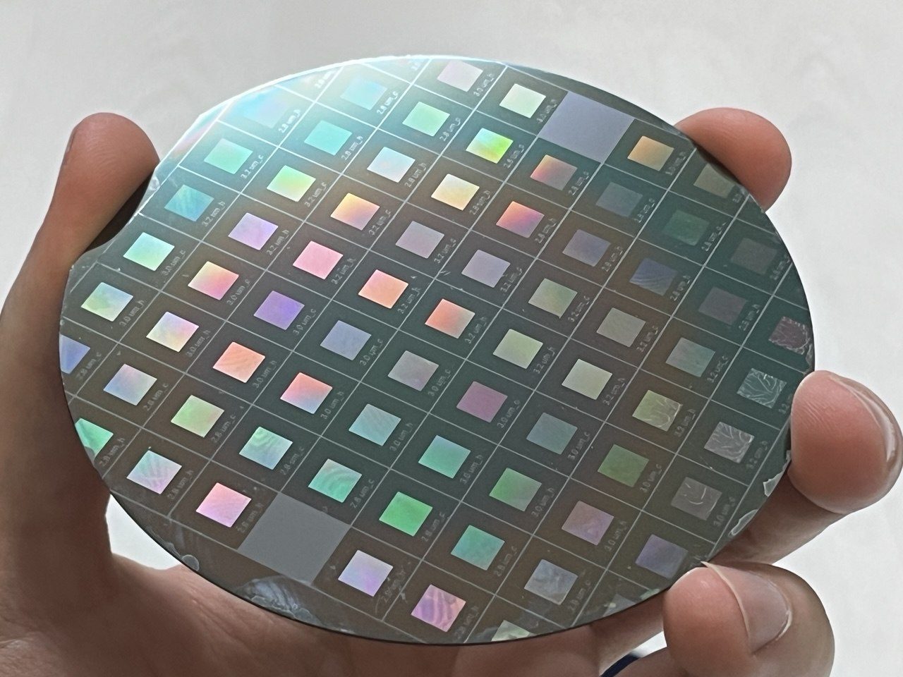
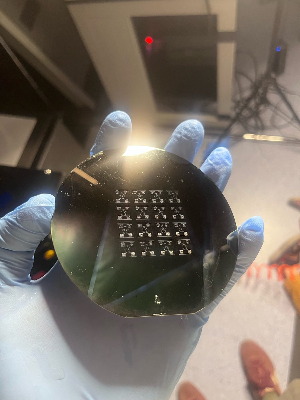
A die array across a whole wafer, stitched by step-and-repeat.
Developed die array.
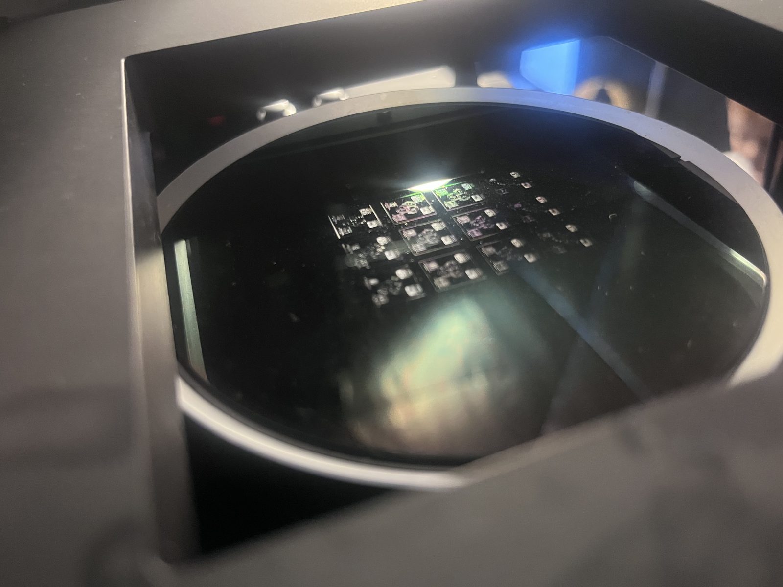
On the chuck, inside the tool.
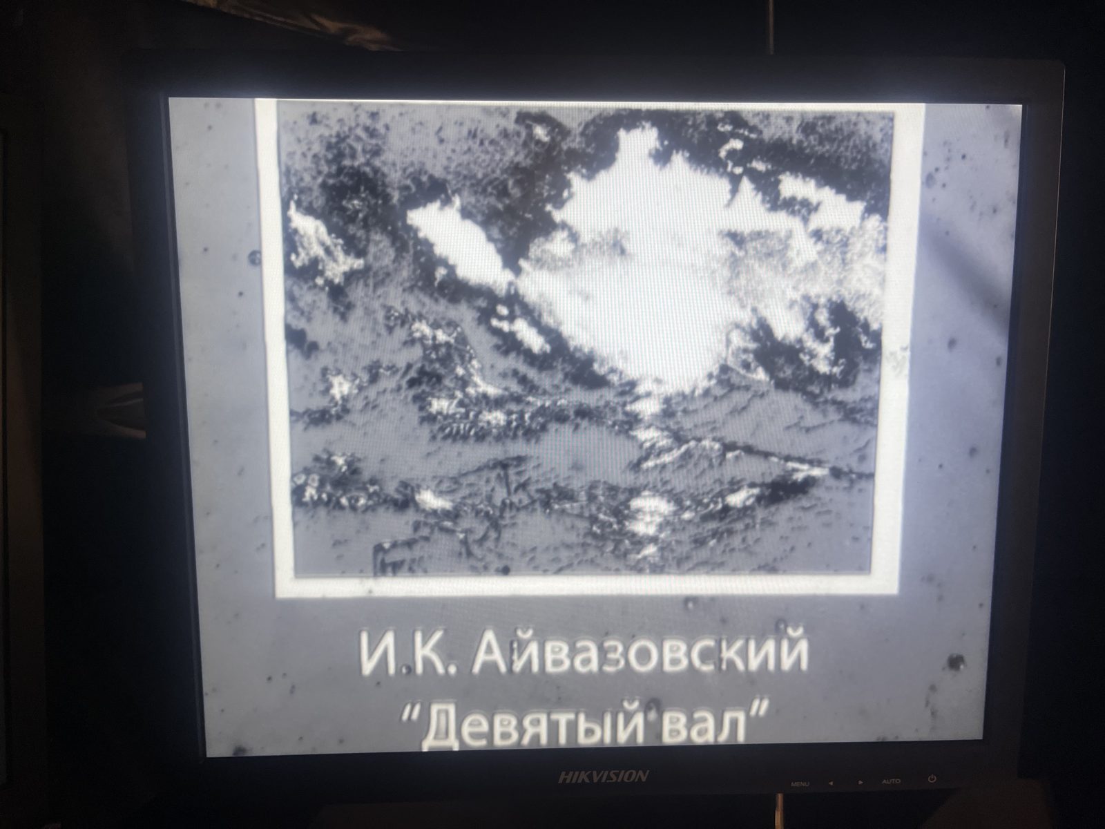
Grey-scale test: Aivazovsky’s “The Ninth Wave” in resist, under the microscope.

Precision from calibration

Sub-micron precision here does not come from granite and air bearings. The machine measures its own geometry and illumination with a camera in the wafer plane and cancels them on every field; the software refuses to expose with an uncalibrated objective.
How the calibration works →

Mask aligner on one side, my maskless prototype on the other.

One engineer

Mechanics, optics, electronics and software — designed, built and brought to working condition by one person.

Other work: portfolio → · CV →

In design

Prototype 2.0

Modular platform · CAD stage

A precision 3-axis motion platform first; lithography is one configuration of it. Three identical linear modules make the XYZ gantry, and everything above the stage bolts to a standard optical-breadboard grid.

Renders with dots are interactive: hover over or tap a part to see what it does.
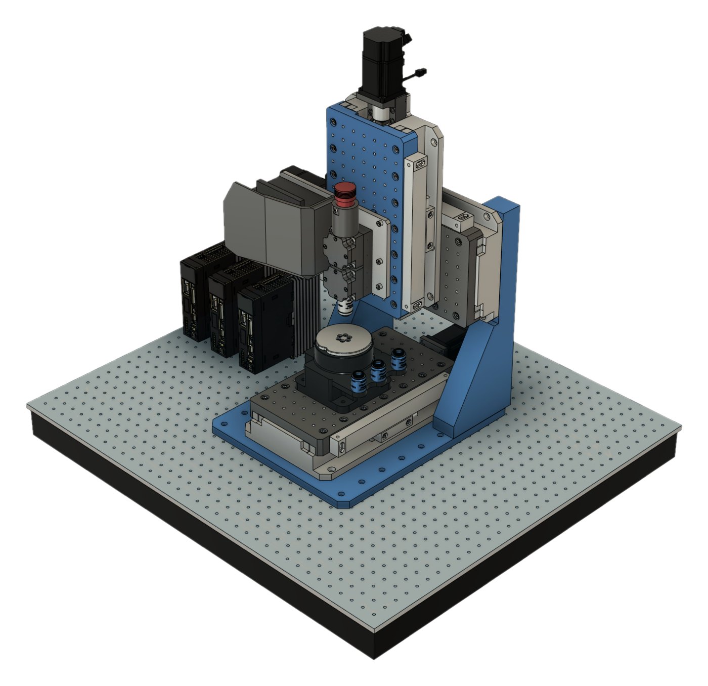
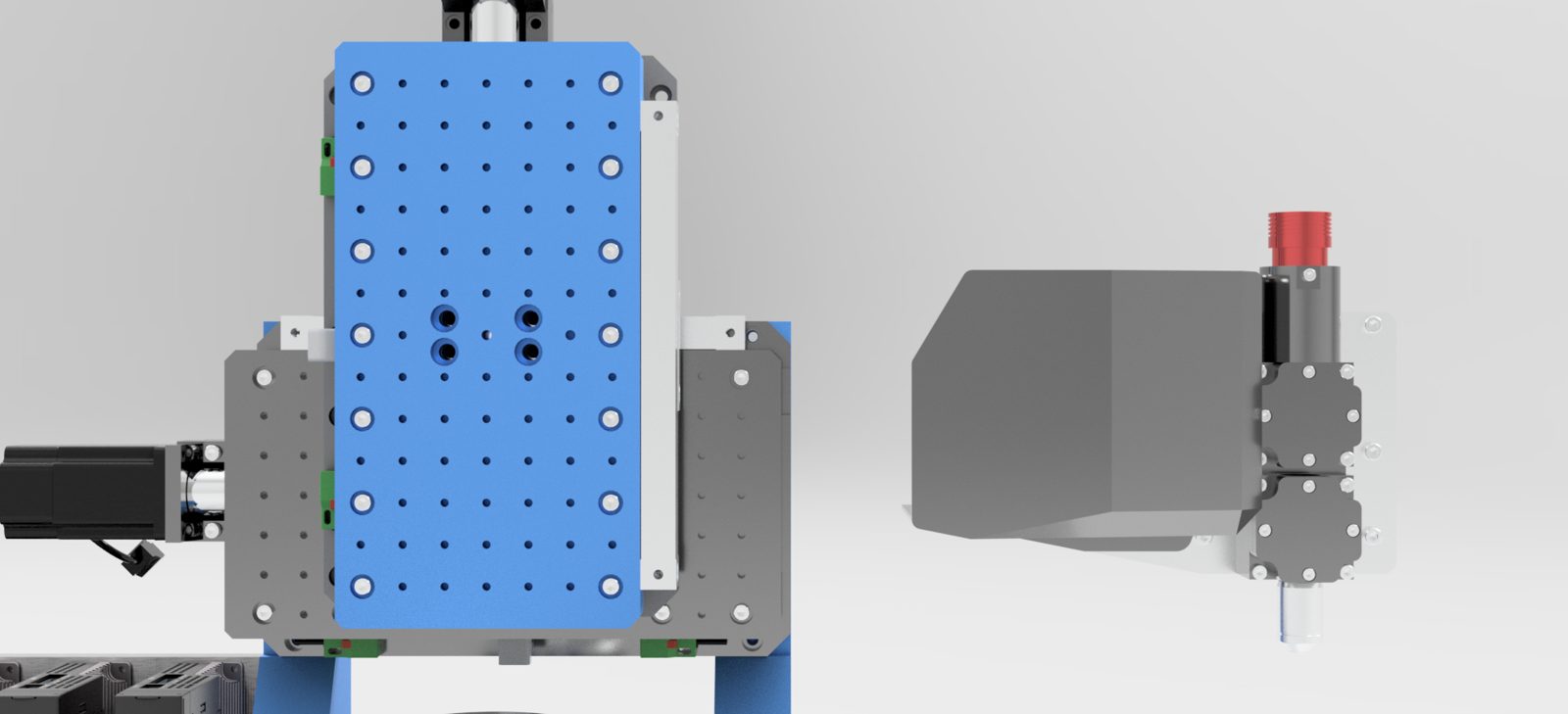
Three copies of the module make the XYZ platform; the head bolts to the Z carriage.
Optical tableA standard breadboard with M6 threads on a 25 mm grid, so ordinary optomechanics mounts right next to the machine.
Gantry frameTwo columns on a base plate carry the gantry axis and bolt down to the optical table.
Stage axisMoves the substrate. The same linear module as above: servo drive, ball screw, crossed-roller guides and an optical scale.
Gantry axisThe second horizontal axis, on the gantry. Together with the stage axis it gives at least 100 × 100 mm of XY travel.
Z axisThe same module mounted vertically: 40 mm of travel for focusing, with the exposure head on its carriage.
Servo drivesOne industrial servo drive per axis, all on a single CANopen bus.
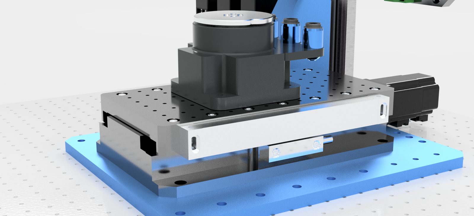
Chuck and objective rackA vacuum chuck on a rotary axis — in development — next to a rack for spare objectives.
Exposure headDMD projection optics with a microscope objective; the camera looks through the same path. The whole head unbolts and can be replaced by other optics.
The whole platform: three copies of one linear module make the XYZ gantry, and the exposure head bolts to the Z carriage. Hover over or tap the dots.

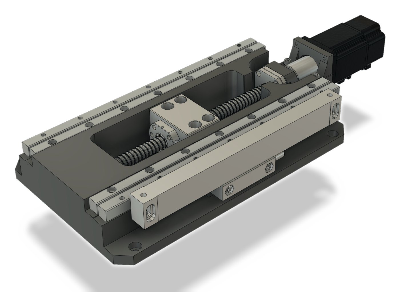
Sub-micron linear module

Every axis is the same block: servo drive, ball screw, crossed-roller guides and an optical scale, closed-loop and complete in itself — 100 nm as standard, 2.5 nm as an option. A product line of its own.
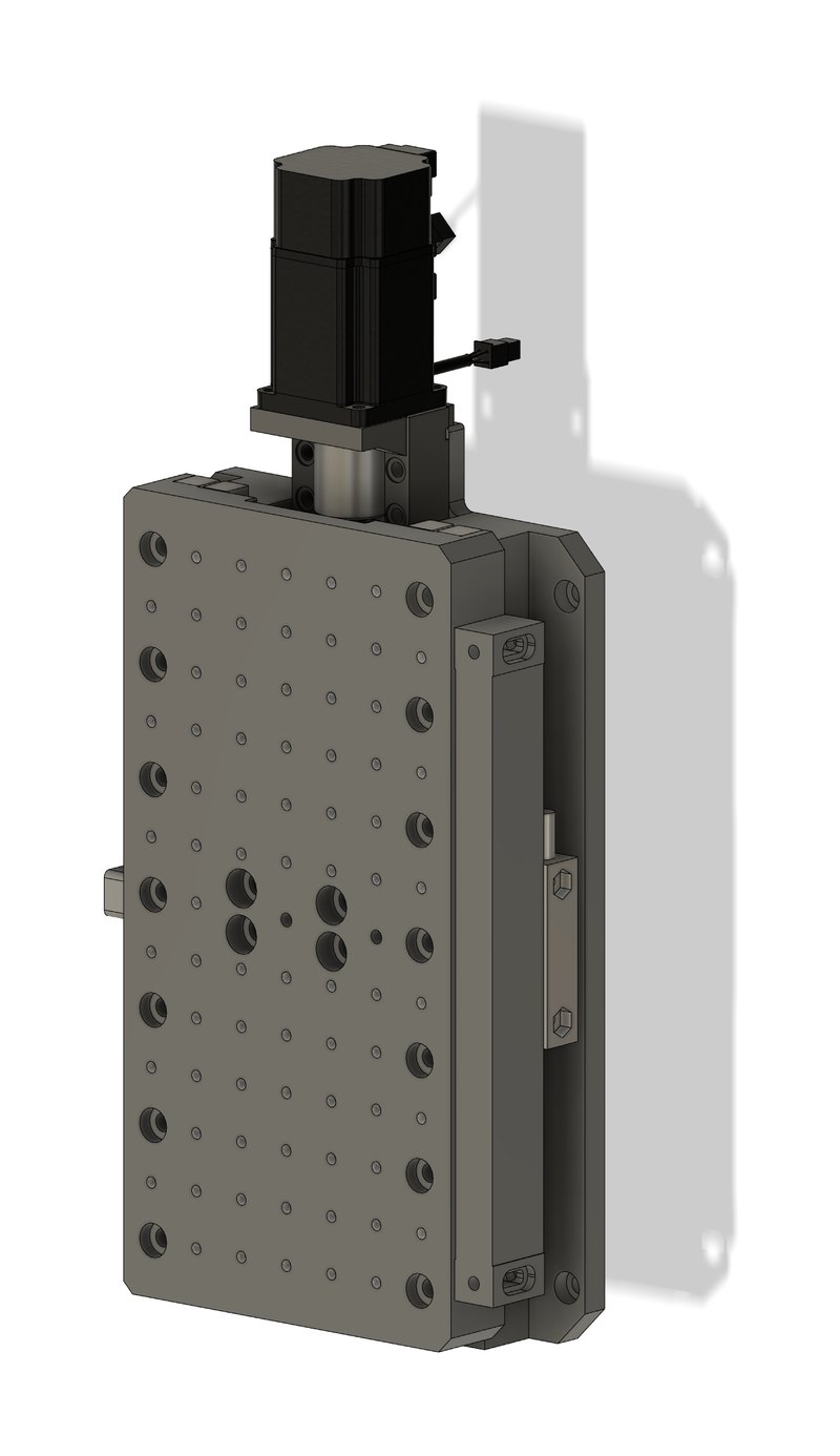
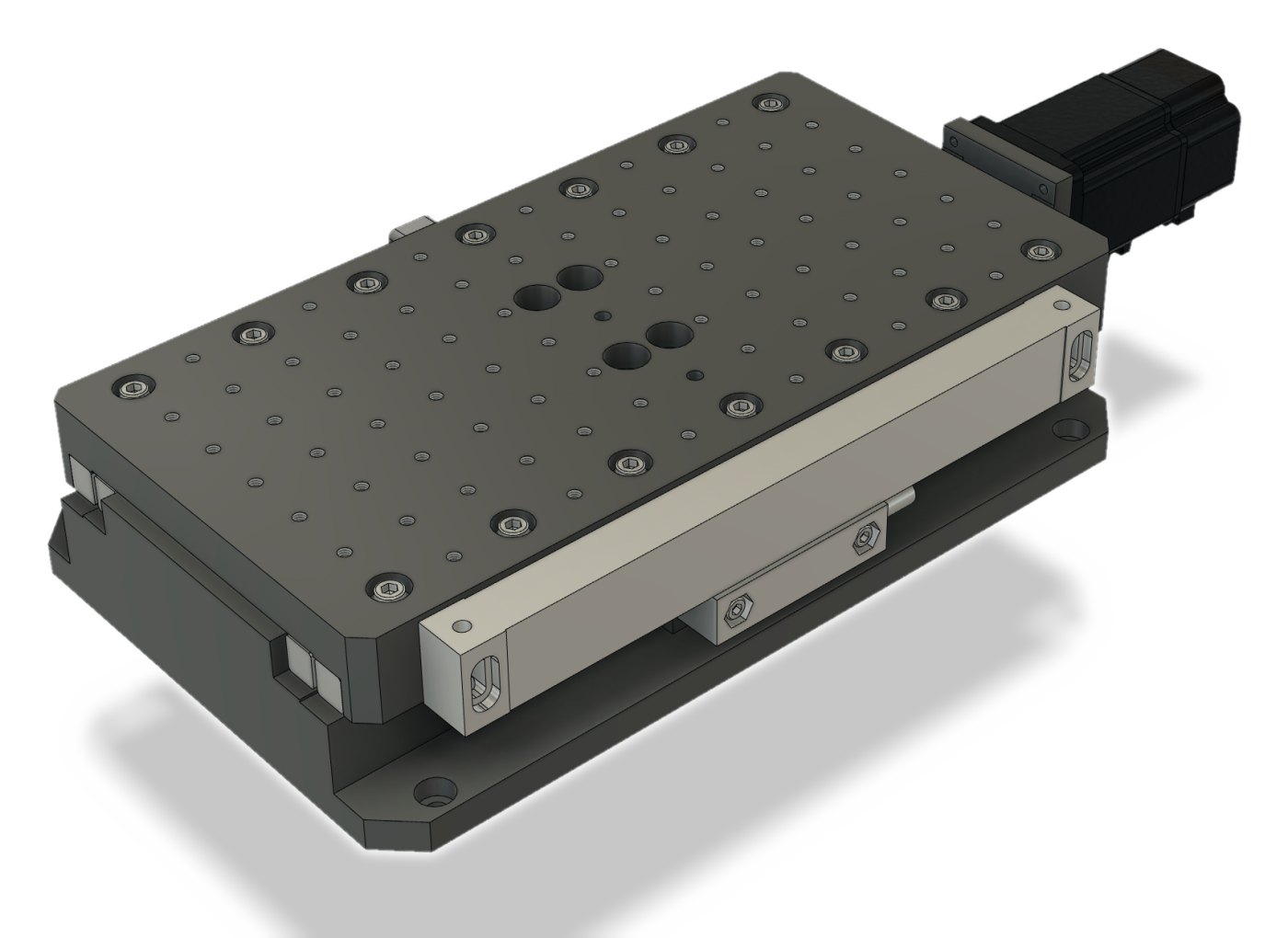
The same module works as the Z axis.
Carriage with a 25 mm / M6 grid.
Base plateMachined base plate that carries the guides and bolts to a table, a frame or another module.
CarriageThe moving table. A 25 mm grid of M6×1 threads takes fixtures, optics or another module directly.
Optical linear scaleA glass scale with a read head measures where the carriage actually is, and the drive closes its loop on that reading — 100 nm as standard, 2.5 nm as an option.
Servo driveAC servo motor on an industrial CANopen bus. It turns the ball screw through a coupling.
Carriage with a 25 mm / M6 grid.
Guides, ball screw and nut.
Base plateMachined base plate that carries the guides and bolts to a table, a frame or another module.
Crossed-roller guidesTwo pairs of crossed-roller rails carry the carriage: stiff, smooth and low in friction.
Ball screw and nutTurns the motor’s rotation into straight travel. The nut sits in a bracket under the carriage; the screw end runs in a fixed bearing support.
Optical linear scaleA glass scale with a read head measures where the carriage actually is, and the drive closes its loop on that reading — 100 nm as standard, 2.5 nm as an option.
Servo driveAC servo motor on an industrial CANopen bus. It turns the ball screw through a coupling.
Guides, ball screw and nut.
Sealed optical scale along the axis.
The exposure head unbolts and swaps for other optics.
Details

Substrate end: chuck and objectives

What changes against Prototype 1.0: an open gantry instead of a box, and every part of the optical path made swappable.
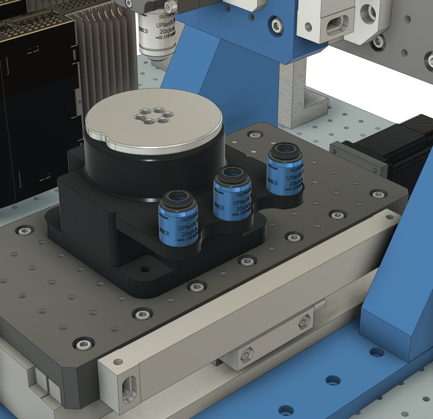
Substrate end
Stage axisMoves the substrate. The same linear module as above: servo drive, ball screw, crossed-roller guides and an optical scale.
Rotary base and objective magazineA compact motor under the chuck will turn the substrate for alignment — in development. The same housing holds the spare objectives.
Vacuum chuckHolds the substrate flat during exposure: silicon up to 4 inches, glass or PCB.
5× objectiveA wide field for finding the substrate and navigating over it.
10× objective10× / 0.5 NA: a larger exposure field per frame.
20× objective20× / 0.75 NA: the finest features, with a smaller field per frame.
The substrate end: chuck and a magazine of 5×, 10× and 20× objectives.
Datasheet

Target specifications

Prototype 2.0. The optical core and software are carried over from Prototype 1.0.

Feature size
0.7–1 µm typicalmin 0.4 µm, optics & resist dependent
Exposure area
100 × 100 mmscalable to 200 × 200 mm
Light source
LED, 440 nm405 nm option · no laser
XY repeatability
0.2 µmclosed loop on optical scales
Position feedback
100 nm scalesdown to 2.5 nm option
Throughput
~2.8 mm²/min @ 1 µm10×; ~0.9 mm²/min @ 0.5 µm (20×)
Light modulator
TI DLP4710 DMD1920 × 1080 micromirrors
Objectives
10× / 0.5 · 20× / 0.75interchangeable
Substrates
Si up to 4″ · glass · PCB
Travel X / Y / Z
≥100 / ≥100 / 40 mm
Design input
GDSII nativeDXF — tuning
Mounting
25 mm grid, M6×1optical-breadboard standard

In development

  • Layer-to-layer alignmentrotary vacuum chuck + alignment workflow in software
  • Automatic objective changemotorized swap between 10× and 20×
  • 405 nm LED optionfor sub-0.5 µm work and broader resist compatibility
  • 2.5 nm optical scalesfor repeatability in the 25–50 nm class

Today it is a single-layer tool: expose, develop, done. If your process needs aligned multilayer now, ask me about the timeline.

Photograph of the exposed test chip, corrected for perspective onto the layout The GDSII layout of the test chip
GDSII layoutIn resist
5 mm
Layout → resist

Design against result

Drag the divider. On the left is the GDSII file that went to the machine; on the right, a photograph of what came out, corrected for perspective so the two line up.

The silicon chip is 25 × 25 mm; the layout on it, a logo with captions and four dithered pictures, takes 20 × 20 mm. One exposure job.

The machine exposes one DMD frame at a time: this chip is 1 869 fields of 0.25 × 0.38 mm, placed side by side by the stage. Switch the picture to Exposure fields and back, and look for the seams.

What ends up in resist depends on development as much as on exposure: developer, time and temperature all change the result. These are samples from process tuning. Works by Magritte and Escher are blurred on both sides: they are still under copyright.

Applications

Where it fits

One base, different instruments

Maskless lithographyDMD head, vacuum chuck, exposure software
Inspection microscopeimaging optics on the same stage
Fluorescence imagingfilters, dichroic, excitation source
Your instrumentprobe stations, laser processing, AOI

Electronics & PCB

Fine-line boards and flex circuits, straight from the layout — same-day iteration.

Microfluidics

Channel networks, master molds for PDMS, on-chip electrodes.

MEMS & sensors

Resist patterns for etching, lift-off and plating on Si up to 4″.

Photonics

Gratings, diffractive elements, waveguide test structures.

Battery R&D

On-chip test cells, microelectrode platforms, microbatteries.

Education & labs

No laser class, compact, enclosed — real workflows from GDSII to wafer.

Software

Written in-house, runs the job from layout to wafer

No third-party CAM chain, no licence dependencies. MVP level: everything below runs on the tool today.
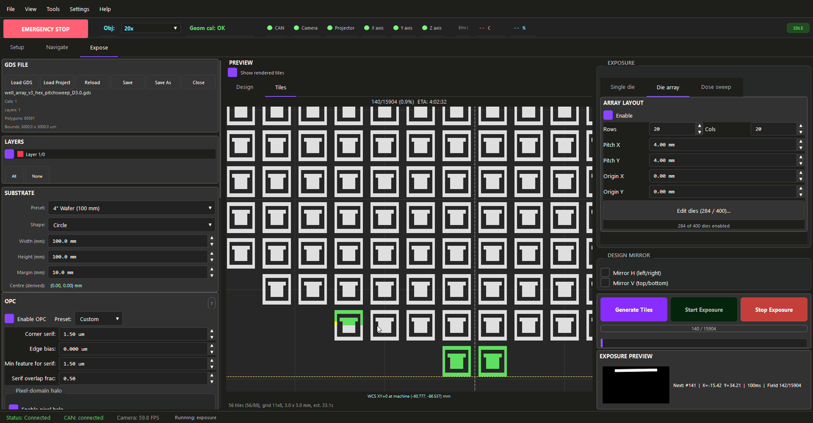
Live wafer map: a 20 × 20 die array, every field coloured as it is exposed.
Contrast autofocus on a height-map point.
Steps of 0.01 / 0.1 / 1 mm over a calibration slide.

What it does

  • Native GDSII import, layers, automatic tiling
  • Die arrays / step-and-repeat
  • OPC assist and focus-exposure matrix
  • Two-phase contrast autofocus under red light
  • Resist-safe illumination: only blue exposes
  • Per-tile exposure time and dose-sweep wafers
  • Substrate height map, per-field Z
  • CANopen servo motion, exposure interlocks
  • Scientific camera pipeline, scale bar per objective
  • Project files with stale-tile detection
Last height-map point → start exposure → watch it on camera.
The Expose tab.
The Expose tab.
Calibration · both prototypes

The machine measures itself

A camera goes on the stage with its sensor facing up, in the plane where the wafer would be. The projector then draws straight onto the sensor, so the software sees exactly what the resist would get — and measures geometry, dose and stitching from it. The same procedure carries over to Prototype 2.0.

The payoff: tolerances move from hardware into software. Parts, rails and optics do not have to be perfect, and the machine does not have to be assembled perfectly — whatever is left is measured and cancelled. That keeps the parts cheaper and the build simpler.

Stacked field grid after calibration: a regular grid Stacked field grid before calibration: tilted squares with uneven gaps
BeforeAfter
500 µm
Before → after

What calibration changes

Drag the divider. Measured sides are camera frames taken in the wafer plane (one sensor pixel is 3.75 µm on the substrate). The compensated side of the white field illustrates the correction algorithm on that same frame.

One square frame exposed at 25 stage positions and stacked into one image. Before: projector rotation against the stage and the rails’ shear show as tilted squares with uneven gaps. After: every move goes through the measured 2 × 2 correction.

Geometry: one 2 × 2 matrix

Projector rotation against the stage, the shear between the X and Y rails and the scale of each axis are measured together and applied to every move. Sub-micron placement at the edge of a 100 mm wafer needs the angle to about 4 arcseconds.

Dose: a per-pixel mask

The camera maps illumination across the field; the software turns it into an attenuation mask on the DMD and adjusts exposure time per tile. The camera then measures the result again, and the mask is refined until the field is flat to within 2–3 %.
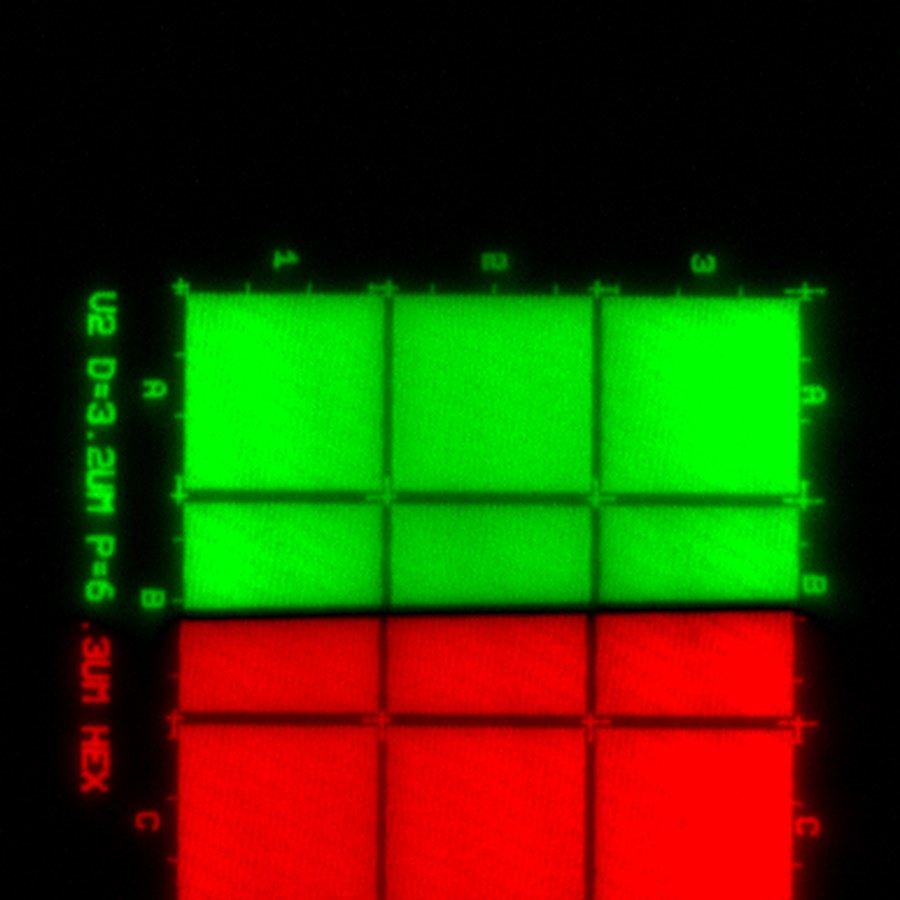
Two neighbouring exposure fields, coloured green and red, meeting on the camera sensor
Stitching check: two neighbouring fields, coloured green and red, meet on the sensor.
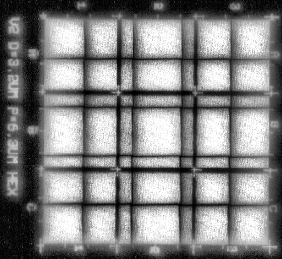
A small mosaic of well-array fields projected onto the camera sensor, with row and column labels
A small mosaic of well-array fields, 3.2 µm wells on a 6.3 µm hex pitch, projected onto the sensor.
Final result · closed loop

Illumination flat to within 2–3 %

ObjectiveBeforeAfterDarkest vs brightest
10×48.7 %97.8 %−2.2 %
20×63.0 %97.9 %−2.1 %
40×70.0 %97.2 %−2.8 %

Uniformity here is the dimmest 2 % of the field — or the darkest corner, whichever is worse — over the brightest 2 %, measured through the objective and averaged over 256 frames. Each objective gets its own mask, refined pass by pass until a pass stops improving it. July–August 2026.
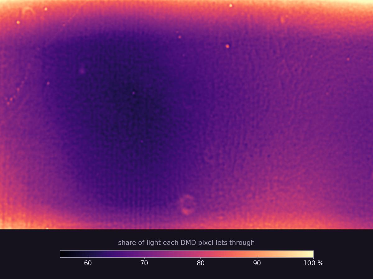
The final uniformity mask for the 10x objective: each DMD pixel dimmed to between 60 and 100 percent
The final 10× mask: where the field was brightest, the DMD dims its pixels to about 60 %; the dimmest areas pass all their light. It is the negative of the illumination.
Progress

How it got here

A year of iterations. The pre-alpha ran on a different projector with a first program written in Windows Forms; Prototype 1.0 got its own stage, its own software and a stitched exposure process.

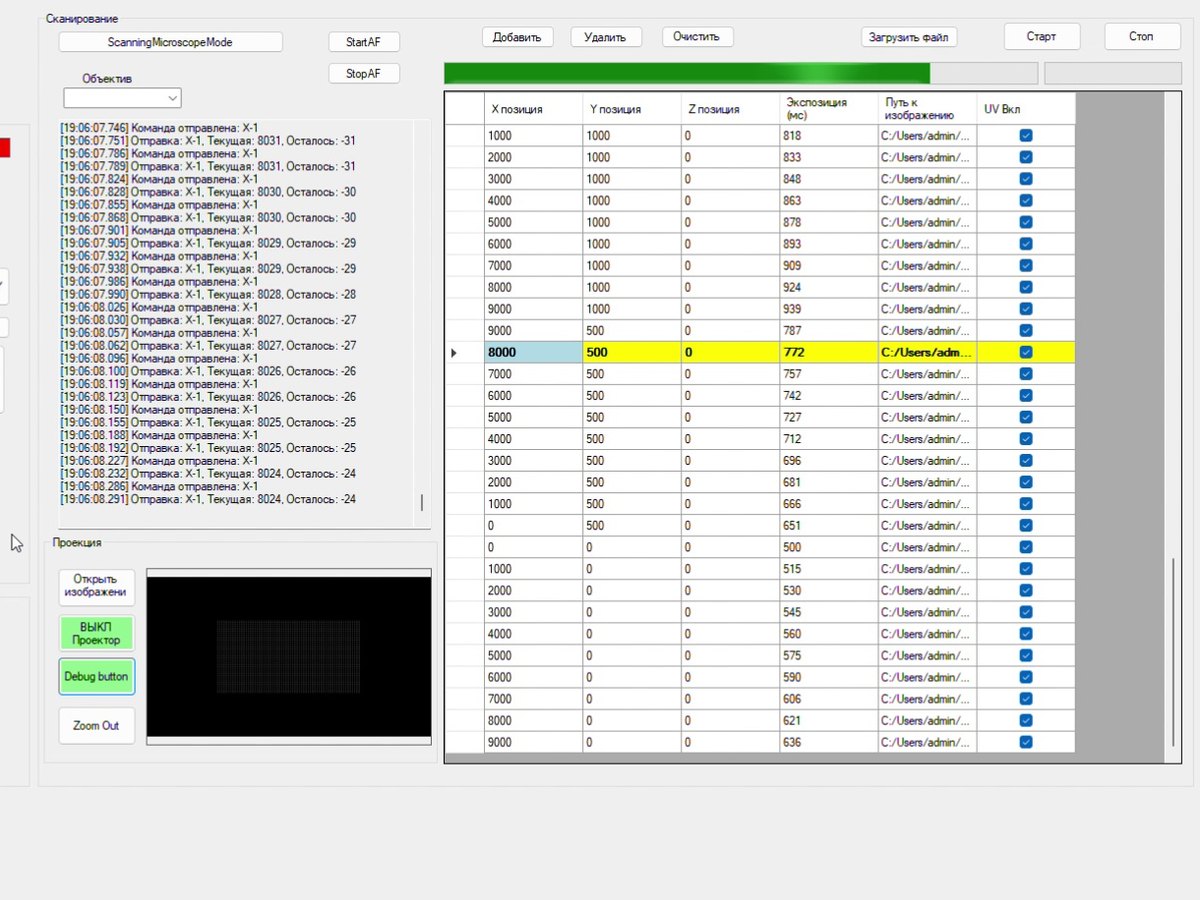
The first control program: a table of stage positions with an exposure time for each field
July 2025 · pre-alpha

The first control program

Windows Forms: a table of fields, each with its own position and exposure time — dose sweeps set up by hand.

Microscope, ×2
July 2025 · pre-alpha

First developed well arrays

Test arrays in resist, each exposed in a single projected field with no stitching, labelled with its own exposure settings.
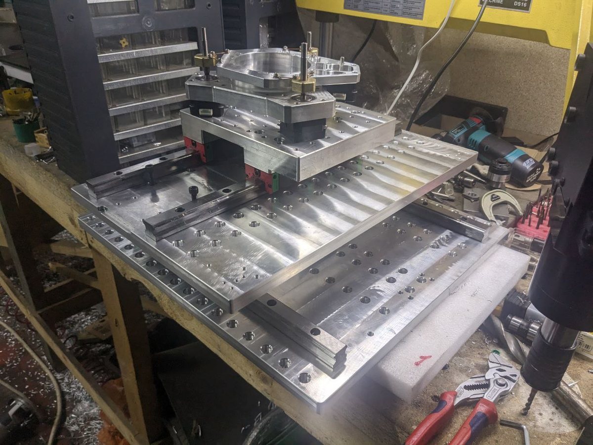
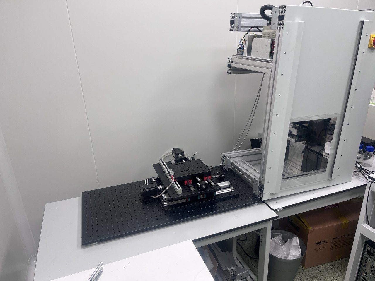
The XY stage with the rotary platform on the bed of a milling machine
Stage rework

Into the milling shop

The XY stage on a milling machine: the rotary platform fitted and the mounting plane machined level.

2026

Prototype 1.0

Its own stage on servo drives and optical scales, the QtLithoCAN software, autofocus and a height map, jobs stitched across whole wafers — everything above on this page.

A test chip made of 1 869 exposure fields shows no visible seams.

Partnership

Looking for a manufacturing partner and investor

On the table: a working Prototype 1.0, the Prototype 2.0 design, full documentation and in-house software. A partner brings production, supply chain and market access; deal structure and investment size are open. Demonstrations and sample exposures by arrangement.